
Copper (I) compounds useful as deposition precursors of copper thin films

a technology of copper and precursors, applied in the field of new copper (i) amidinates, can solve the problems of poor adhesion of metals and high contact resistance, and achieve the effect of improving adhesion

Active Publication Date: 2007-01-23
ROHM & HAAS ELECTRONICS MATERIALS LLC
View PDF25 Cites 18 Cited by
  • Summary
  • Abstract
  • Description
  • Claims
  • Application Information

AI Technical Summary

Benefits of technology

The new copper precursors provide copper thin films with enhanced adhesion and low resistivity, enabling the formation of high-performance copper interconnects in microelectronic devices, particularly in VLSI and thin-film applications, with improved reproducibility and conformality, suitable for next-generation device geometries.

Problems solved by technology

In instances where (hfac)CuL type precursors are used for copper metallization, interfacial layers are formed between the barrier layer and the copper layer, which cause the metallization to have poor adhesion and high contact resistivity.

Method used


Image

  • Copper (I) compounds useful as deposition precursors of copper thin films
  • Copper (I) compounds useful as deposition precursors of copper thin films
  • Copper (I) compounds useful as deposition precursors of copper thin films

Examples


example 1

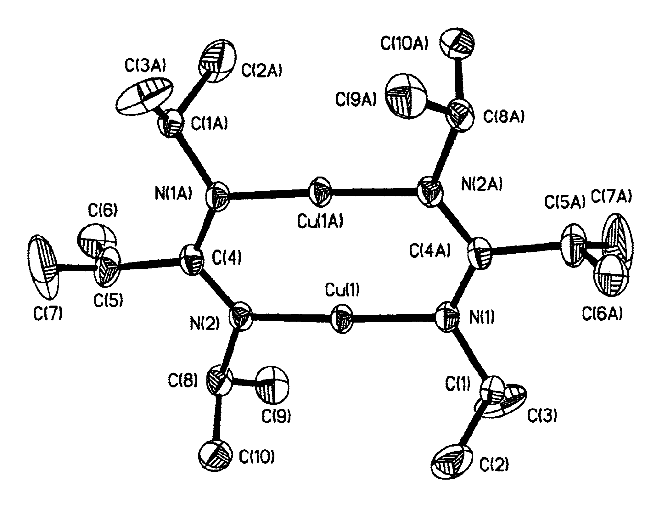
Synthesis of copper (I) 2-isopropyl-1,3-diisopropylamidinate

[0050]The reaction was carried out under a steady flow of nitrogen. A Schlenk flask was charged with 6.3 g of 1,3-diisopropylcarbodiimide ((CH3)2CHN═C═NCH(CH3), 49.9 mmol) and 50 mL dry ether and placed in an ice bath. Then, 32 mL of isopropyllithium (1.6M in ether, 51.2 mmol) was added dropwise to the magnetically stirred mixture at about 0° C. After the addition was complete, the mixture was stirred at room temperature for two additional hours. The mixture was transferred to another flask containing 6 g of CuCl (60.6 mmol) suspended in 50 mL ether. This mixture was stirred at room temperature overnight and then stripped to dryness. The solid residue was extracted with pentane (3×50 mL). After extraction, the pentane filtrate was concentrated to slightly cloudy. The saturated solution was placed in a freezer at −39° C., and crystalline product was obtained in a yield of about 60%.

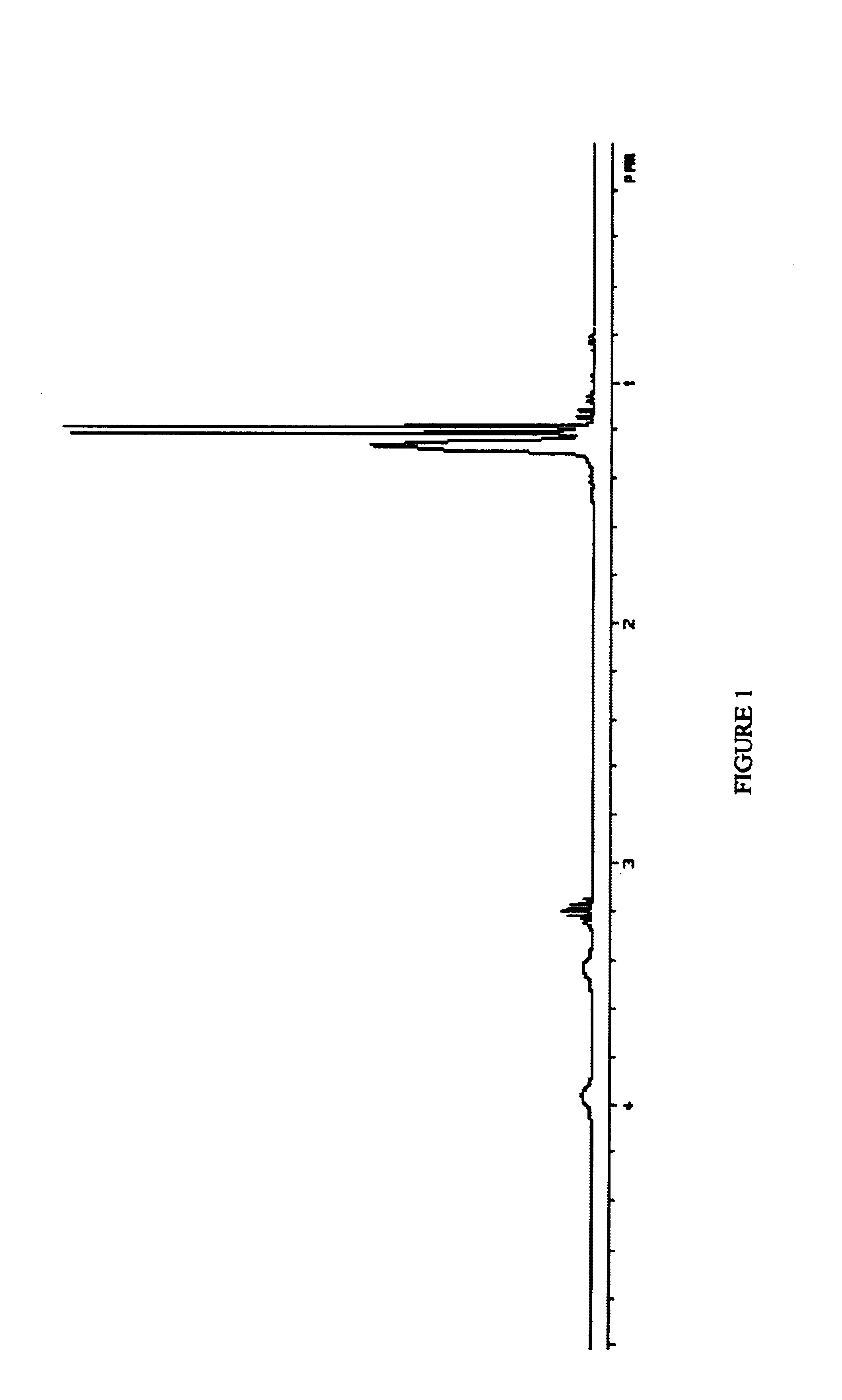
[0051]FIG. 1 shows the 1H NMR (C6D6) for co...

example 2

Synthesis of copper (I) 2-dimethylamino-1,3-diisopropylamidinate

[0054]Neat 1,3-diisopropylcarbodiimide (12.37 g, 98 mmol, 15.2 mL) was slowly added to a solution of LiNMe2 (5 g, 98 mmol) in 125 mL of THF. Some heat generation was observed. The reaction mixture was stirred for 1 hour. Thereafter, 9.7 g of solid CuCl (98 mmol) was added to the reaction mixture in a dry box. The resulting greenish suspension was stirred overnight and all volatiles were removed in vacuum. The residue was washed in 150 mL of hexane. Filtrate was concentrated in vacuum and placed in a refrigerator whereby neat crystals grew overnight. The overall yield was 60% and the melting point of the crystals was 108° C. 1H NMR (C6D6): δ 3.42 (septet, 1H, J(H—H)=6 Hz, CH(CH3)2), 2.55 (singlet, 3H, N(CH3)2), 1.30 (doublet, 6H, J(H—H)=6 Hz, CH(CH3)2). 13C NMR (C6D6): δ 171.95 (Me2NC(iPr))2), 48.61 (CH(CH3)2), 41.29 (N(CH3)2), 27.98 (CH(CH3)2).

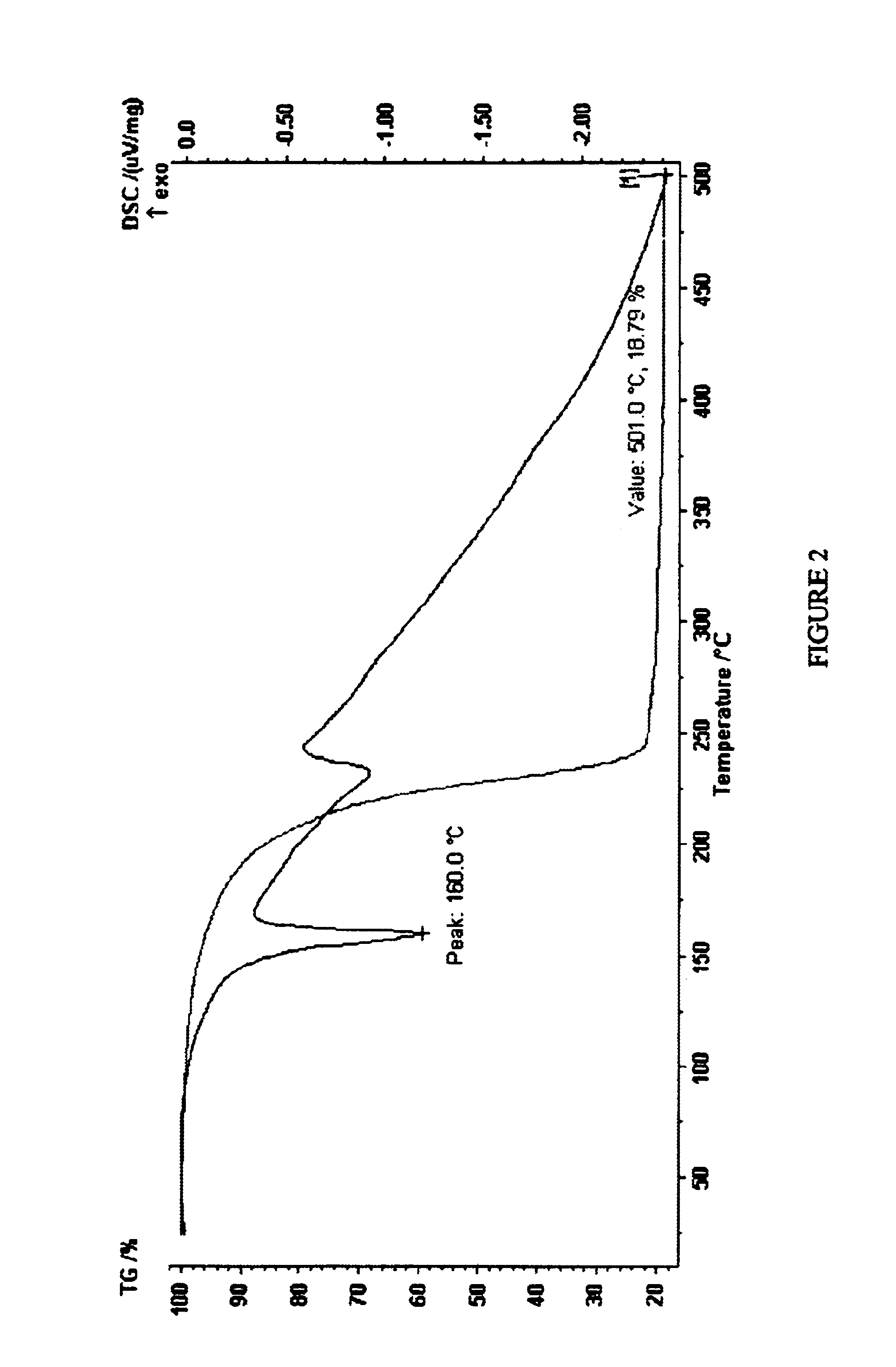
[0055]FIG. 4 shows the STA / DSC plot for copper (I) 2-dimethylamino-1,3-diisop...


PUM

PropertyMeasurementUnit
temperatureaaaaaaaaaa

Abstract

Copper (I) amidinate precursors for forming copper thin films in the manufacture of semiconductor devices, and a method of depositing the copper (I) amidinate precursors on substrates using chemical vapor deposition or atomic layer deposition processes.

Description

FIELD OF THE INVENTION[0001]The present invention relates generally to novel copper (I) amidinates and their synthesis, and to a method for production of copper circuits in microelectronic device structures using the novel copper precursors.DESCRIPTION OF THE RELATED ART[0002]As a result of its low resistivity, low contact resistance, and ability to enhance device performance through the reduction of RC time delays, copper has emerged as a preferred metal for metallization of very large scale integrated (VLSI) devices. Copper metallization has been adopted by many semiconductor device manufacturers for production of microelectronic chips, thin-film recording heads and packaging components.[0003]Chemical vapor deposition (CVD) of copper provides uniform coverage for the metallization. Atomic layer deposition (ALD), which is a modified CVD process, also provides uniform coverage which is critical for copper seed layers. Liquid CVD precursors and / or solid precursors dissolved into solv...

Claims


Application Information

Patent Timeline
Patent Type & Authority Patents(United States)
IPC IPC(8): C07F1/00C07F1/08C07C257/14C23C16/00C23C16/18
CPCC07C257/14C23C16/18C07F1/005C07F1/08C23C16/00
Inventor XU, CHONGYINGBOROVIK, ALEXANDERBAUM, THOMAS H.
Owner ROHM & HAAS ELECTRONICS MATERIALS LLC
Learn More