Method for removing photoresist and etch residues

Inactive Publication Date: 2007-01-30
TOKYO ELECTRON LTD
View PDF21 Cites 20 Cited by
  • Summary
  • Abstract
  • Description
  • Claims
  • Application Information

AI Technical Summary

Benefits of technology

[0013]During the first ashing step, where low or zero bias is applied to the substrate, a significant amount of photoresist remnants and etch residues on the substrate and internal surfaces/walls of the process chamber are etched and remov

Problems solved by technology

In semiconductor processing, where various types of films are etched, integration challenges and trade-offs still remain.
One of the integration challenges in plasma cleaning (also known as in-situ ashing), is to successfully remove photoresist remnants and etch residues, while avoiding erosion of surrounding layers.
As bias i

Method used


Image

  • Method for removing photoresist and etch residues
  • Method for removing photoresist and etch residues
  • Method for removing photoresist and etch residues

Examples


Embodiment Construction

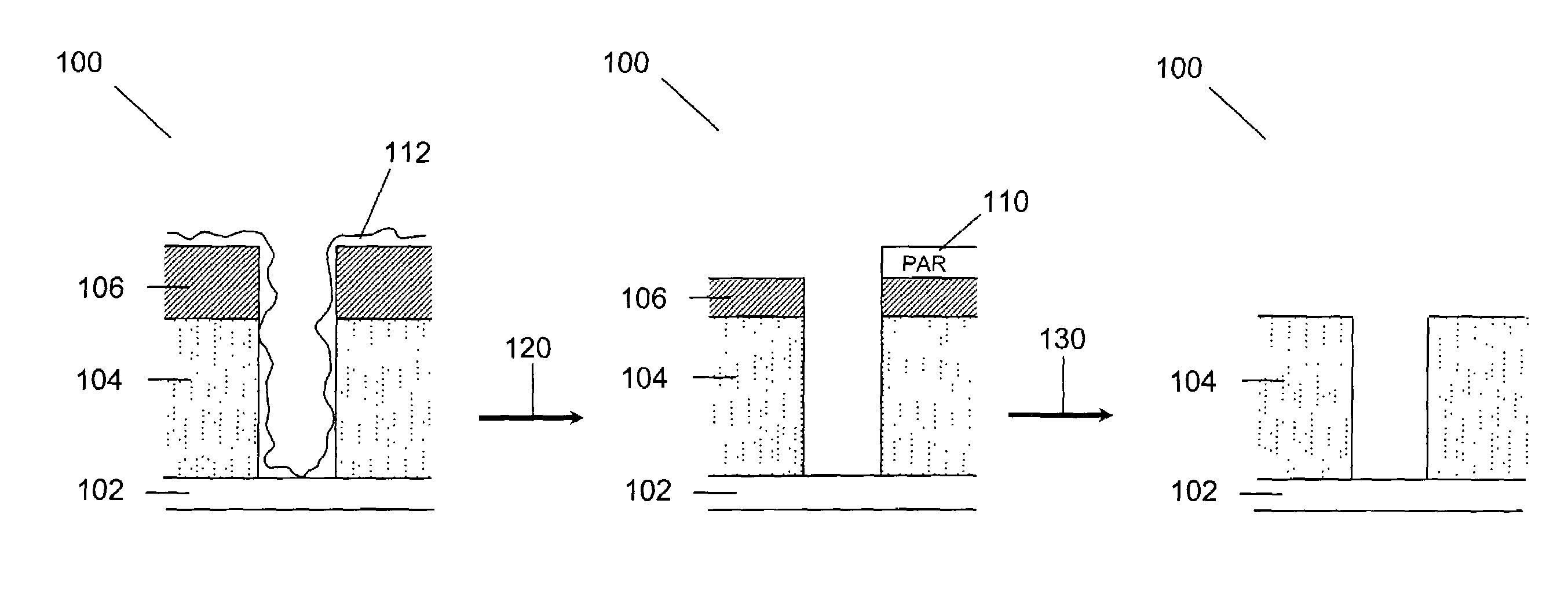
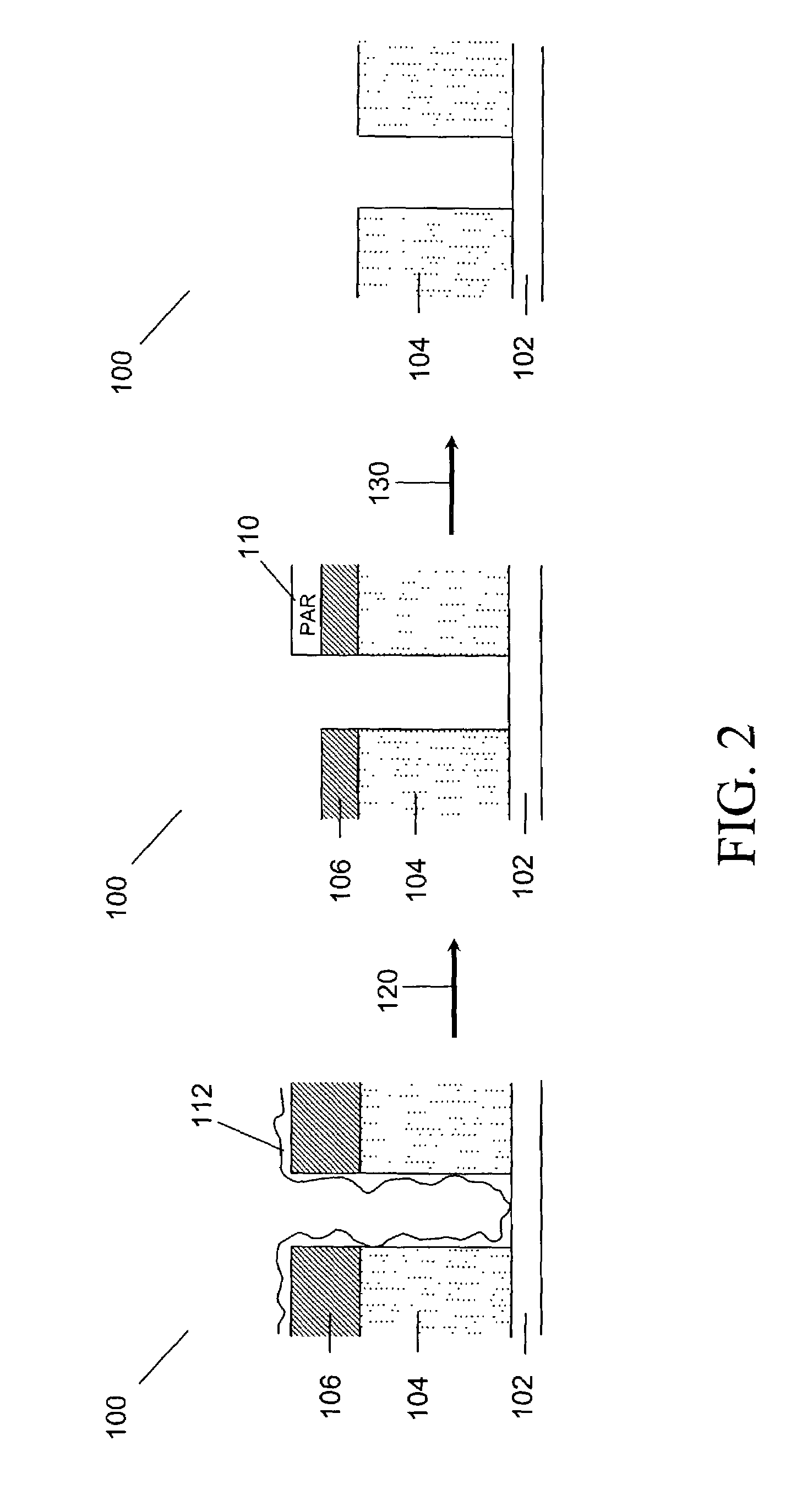
[0020]In one embodiment of the invention, a two-step plasma ashing process is utilized to remove photoresist remnants and etch residues from a processing chamber. During the first ashing step, where zero or low bias is applied to a substrate holder upon which a substrate resides, a significant amount of photoresist remnants and etch residues, from a preceding etch process, are etched and removed from the chamber with minimal erosion of the remaining substrate layers. During the second ashing step, an increased bias is applied to the substrate holder and the ashing process is continued until the photoresist and / or hard mask remnants, and post-ash residues are removed.

[0021]A two-step in-situ ash process in the current invention can alleviate many of the above shortcomings by satisfying at least one of: 1) minimizing cap layer consumption; 2) minimizing dielectric faceting / erosion at the top of features, and reducing post-etch / critical-dimension (CD) bias; 3) minimizing post-ash resid...


PUM

PropertyMeasurementUnit
Pressureaaaaaaaaaa
Pressureaaaaaaaaaa
Pressureaaaaaaaaaa

Abstract

A method is provided for plasma ashing to remove photoresist remnants and etch residues that are formed during preceding plasma etching of dielectric layers. The ashing method uses a two-step plasma process involving an oxygen-containing gas, where low or zero bias is applied to the substrate in the first cleaning step to remove significant amount of photoresist remnants and etch residues from the substrate, in addition to etching and removing detrimental fluoro-carbon residues from the chamber surfaces. An increased bias is applied to the substrate in the second cleaning step to remove the remains of the photoresist and etch residues from the substrate. The two-step process reduces the memory effect commonly observed in conventional one-step ashing processes. A method of endpoint detection can be used to monitor the ashing process.

Description

CROSS-REFERENCE TO RELATED APPLICATIONS[0001]The present application is related to and claims priority to U.S. provisional application serial No. 60 / 372,446 filed on Apr. 16, 2002, the entire contents of which are herein incorporated by reference. The present application is related to co-pending U.S. patent application Ser. No. 10 / 259,381,entitled “Method for removing photoresist and etch residues”, filed on even date herewith, the entire contents of which are herein incorporated by reference.FIELD OF THE INVENTION[0002]The present invention is related to plasma processing, particularly to cleaning and removal of photoresist and etch residues following an etch process in semiconductor microfabrication.BACKGROUND OF THE INVENTION[0003]Plasma processing systems are used in the manufacture and processing of semiconductors, integrated circuits, displays, and other devices or materials to both remove material from or to deposit material on a substrate such as a semiconductor substrate. P...

Claims


Application Information

Patent Timeline
IPC IPC(8): B05D5/06B31D3/00H01L21/3065G03F7/42H01L21/02H01L21/027H01L21/304H01L21/311
CPCH01L21/31138H01L21/02063G03F7/427H01L21/3065H01L21/304
Inventor BALASUBRAMANIAM, VAIDYANATHANHAGIWARA, MASAAKINISHIMURA, EIICHIINAZAWA, KOUICHIRO
Owner TOKYO ELECTRON LTD
Why Eureka
Try Eureka