Methods of Minimizing Etch Undercut and Providing Clean Metal Liftoff

a technology of etching substrate and clean metal, which is applied in the field of etching substrate methods, can solve the problems of difficult dimension control, limited total thickness of metal that can be deposited on the etched surface, and difficult and straightforward selection of all metal layers in the “etch-back” approach, etc., and achieves short etch time, high etch selectivity, and adequate step coverage

Active Publication Date: 2009-04-30
TRIQUINT SEMICONDUCTOR
View PDF11 Cites 25 Cited by
  • Summary
  • Abstract
  • Description
  • Claims
  • Application Information

AI Technical Summary

Benefits of technology

[0024]Of one advantage, the present invention avoids any effect associated with the layer intermixing between the bottom and top resist layers. The use of plasma etching such as oxygen RIE in the present invention to remove the exposed portion of the bottom resist using the top photoresist as the etch mask also etches away any intermixed interfacial layer between the two resist layers.
[0025]Further, in some embodiments, the present invention provides adequate step coverage on highly non-planar substrate surfaces by using a relatively thin bottom and a relatively thick top resist layers for substrate etching and metal liftoff. This is in contrast to prior art techniques in which the bottom resist layer is relatively thick and used primarily as a planarization layer and rely on high etch selectivity of the bottom resist over the top masking material comprising another photoresist, spin on glass or metal in oxygen plasma. The present invention utilizes a relatively thin bottom resist layer for the formation of an overhang resist edge profile following the etching of the exposed portion of the underlying substrate material. Step coverage and planarization are accomplished primarily through the use of a relatively thick top photoresist layer. An advantage of this method is that only a relatively short etch time is needed to completely remove the exposed portion of the bottom resist in the top photoresist opening during etching or exposure, thereby minimizing the erosion of the top photoresist mask.
[0026]In another aspect, embodiments of the present invention provide methods of further minimizing the etch undercuts around the deposited metal pattern on the etched substrate surface by first introducing a dielectric layer of good adhesion to the substrate material prior to applying the bilayer resist process described above in the present invention. As described above, in some embodiments the invention comprises a bottom resist directly in contact with the underlying substrate material. The etch undercuts are determined by the adhesion of the bottom resist to the underlying substrate material and the etch depth. Organic resist materials generally do not adhere well to a semiconductor substrate surface, leading to large etch undercuts. In one preferred embodiment of the present invention, an extra layer of dielectric material such as silicon nitride is first deposited using standard deposition methods such as plasma enhanced chemical vapor deposition (PECVD) on top of the substrate material prior to formation of the bottom and top resists. In some embodiments the bottom and top resist layers are formed by spinning and coating techniques known in the art. A patterned bilayer resist stack structure without the resist overhang is next formed similar to the method described above in the present invention and is then used as the etch mask for etching of the exposed portion of the dielectric layer through the bilayer resist opening. This is followed by a blanket exposure without a mask with deep UV irradiation and development of the exposed sidewalls of the bottom resist around the bottom resist opening in a second developer, which does not dissolve the exposed top photoresist to create bottom resist undercuts and an overhang resist edge profile in the bottom resist layer useful for subsequent clean metal liftoff. Etching of the dielectric layer can be performed isotropically or anisotropically by wet or dry etching. The dielectric layer provides good adhesion to the underlying substrate material and thus minimizes the etch undercuts of the underlying substrate material around the deposited metal pattern on the etched substrate surface.
[0027]In another aspect of the present invention methods of sealing the etch undercut regions around the deposited metal on the etched substrate surface are provided. Sealing of the etch undercut regions on the substrate protects the regions from being chemically attacked in subsequent wafer processing. In some embodiments sealing is accomplished through the addition of an oxygen plasma etching step such as oxygen RIE or descum following the etching of the exposed portion of the dielectric layer in the bilayer resist opening. The additional oxygen plasma etching widens the top photoresist opening to an extent such that the top photoresist opening is larger than the dielectric opening. When etching of the exposed portion of the underlying substrate is complete, the entire wafer is next blanket exposed without a mask. Blanket exposure may be accomplished by any suitable means, for example without limitation by deep UV irradiation. The sidewalls of the bottom resist in the bottom resist opening are then developed in a developer, which does not dissolve the exposed top photoresist, to create bottom resist undercuts. This is followed by metal deposition by means of metal evaporation or sputter deposition method. Because of the presence of the bottom resist undercuts and the larger size of the top photoresist opening, some of the metal is also deposited on the exposed portion of the dielectric layer around the dielectric opening. When the total thickness of the deposited metal is larger than the combined thickness of the dielectric layer and the etch depth of the underlying substrate, the deposited metal on the etched substrate surface is connected to the deposited metal on top of the dielectric layer around the dielectric opening, thereby sealing the etch undercut regions on the substrate from the outside environment.
[0028]Embodiments of the present invention advantageously provides a method for creating a liftoff resist structure for clean metal liftoff with minimized etch undercut regions of etched substrate material in a bilayer resist process involving substrate etching. Moreover embodiments of the present invention advantageously provide methods for allowing large bottom layer resist undercuts to assist metal liftoff in a bilayer resist process involving substrate etching. Further, methods provide improved resist step coverage over a highly non-planar substrate surface for metal liftoff in a bilayer resist process.
[0029]In another aspect, embodiments of the present invention advantageously provide methods for sealing the etch undercut regions of etched substrate material with metal in a bilayer resist process involving substrate etching and protecting the regions from chemical attacks in subsequent wafer processing or from the environment.

Problems solved by technology

The “liftoff” technique allows easy creation of metal patterns comprising different metal layers whereas selective removal of all the metal layers in the “etch-back” approach is not always easy and straightforward.
However, a drawback of negative photoresists is the swelling of resist around the development pattern, which makes the dimension control difficult.
This limits the total thickness of the metal that can be deposited on the etched surface.
It is a disadvantage of this approach that makes use of a resist edge profile with such a negative slope around the photoresist opening in etching prior to metal deposition if one of the requirements is to minimize the laterally etched regions 222 and 224 around the deposited metal 220 on the etched substrate surface 212.
It is a disadvantage of this approach that makes use of a photoresist edge profile with such an overhang around the photoresist opening in etching prior to metal deposition if one of the requirements is to minimize the laterally etched regions 322 and 324 around the deposited metal 320 on the etched substrate surface 312.
It is a disadvantage of this approach that makes use of such a re-entrant resist edge profile around the photoresist opening in etching prior to metal deposition if one of the requirements is to minimize the laterally etched regions 422 and 424 around the deposited metal 420 on the etched substrate surface 412.
Another known problem in this approach is the difficulty in controlling of the amount of photoresist undercuts 404 and 406 in the re-entrant resist edge profile.
These methods, however, generally do not result in sufficient resist overhangs needed for clean metal liftoff for a thick metal layer and the resultant bilayer resist edge profile is similar to that in the prior art that utilizes a single layer of positive photoresist described earlier and illustrated in FIGS. 1a to 1d.
It is a disadvantage of this approach that makes use of a bilayer resist process with such an overhang resist edge profile in etching prior to metal deposition if one of the requirements is to minimize the laterally etched regions 522 and 524 around the deposited metal 530 on the etched substrate surface 512.
However, such techniques require the use of a separate, expensive electron beam lithography tool and lose the advantage of doing all mask patterning steps all optically with a conventional photolithography tool such as a stepper or a mask aligner.
However, such methods have limitations.
When resist overhangs or undercuts are present, however, the subsequent etch undercuts of the underlying substrate around the deposited metal pattern on the etched substrate surface are naturally large compared to ones with straight resist sidewalls.

Method used


Image

  • Methods of Minimizing Etch Undercut and Providing Clean Metal Liftoff
  • Methods of Minimizing Etch Undercut and Providing Clean Metal Liftoff
  • Methods of Minimizing Etch Undercut and Providing Clean Metal Liftoff

Examples


first embodiment

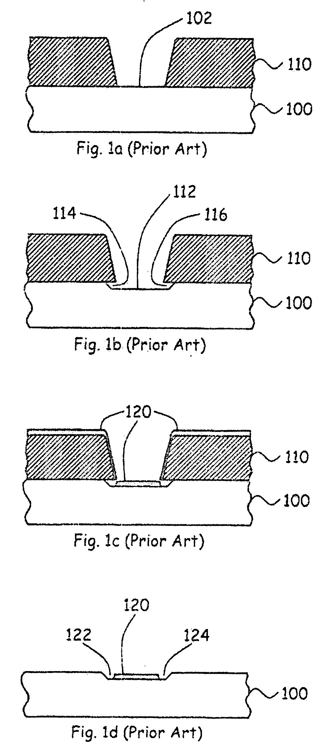
[0046]Subsequent creation of the resist overhang structure for facilitating clean metal liftoff follows a procedure similar to that described above in the present invention. After the etching of the exposed portion 732 of the substrate 700, the entire wafer with the bilayer resist pattern is then blanket exposed without a mask with deep UV irradiation. This exposes the sidewalls of the bottom resist opening to the deep UV light. The sidewalls of the bottom resist opening are next developed in a second developer, which does not dissolve the exposed top layer photoresist 730. If the bottom resist 720 is PMMA and is etched earlier by the means of oxygen RIE, it may not be necessary to use the blanket exposure with deep UV irradiation to expose the sidewalls of the PMMA because the light emission from the oxygen plasma contains light of wavelengths that can expose the PMMA. One such second developer that develops exposed PMMA but not the top photoresist is toluene. The exposure of the s...

second embodiment

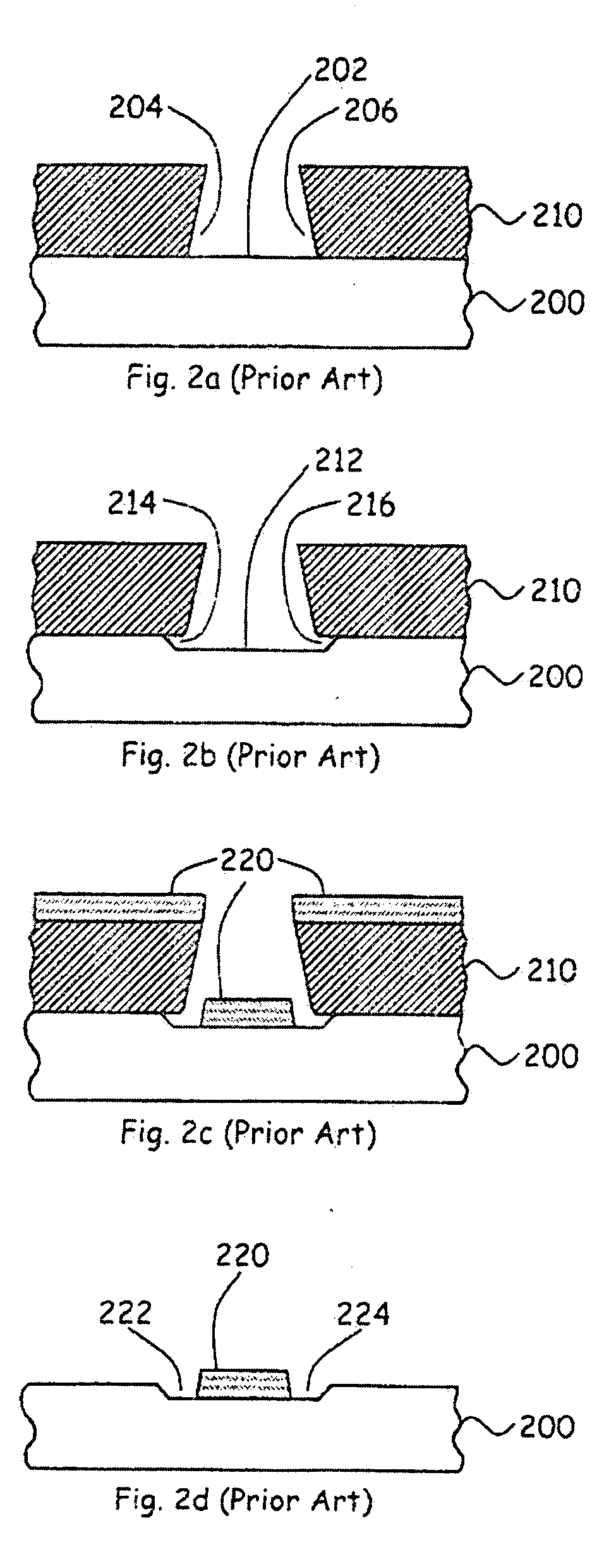
[0053]Following creation of an overhang resist edge profile in the bilayer resist structure, a metal evaporation or sputter deposition step is next performed to deposit the desired metal 870 on the wafer as illustrated in FIG. 8l. The total deposited metal thickness is to be larger than the combined etch depth of the underlying substrate and the thickness of the dielectric layer 810, but is to be smaller than the thickness of the bottom resist layer 820 for clean metal liftoff. Because the top photoresist opening is larger than the dielectric opening after going through the earlier pattern widening step of the resist opening and because the bottom resist has undercuts 864 and 866, metal is also deposited on top of the exposed portions of the dielectric layer around the dielectric opening. When the total thickness of the deposited metal 870 is larger than the combined etch depth of the substrate material and the thickness of the dielectric layer 810, the deposited metal 870 on the et...


PUM

PropertyMeasurementUnit
wavelengthaaaaaaaaaa
thicknessaaaaaaaaaa
wavelengthaaaaaaaaaa

Abstract

A method of minimizing etch undercut and providing clean metal liftoff in subsequent metal deposition is provided. In one embodiment a bilayer resist mask is employed and used for etching of underlying substrate material and subsequent metal liftoff. In one embodiment, the top layer resist such as positive photoresist which is sensitive to selected range of energy, such as near UV or violet light, is first patterned by standard photolithography techniques and resist development in a first developer to expose portion of a bottom resist layer which is sensitive to a different selected range of energy, such as deep UV light. The exposed portion of the bottom layer resist is then removed by anisotropic etching such as oxygen reactive ion etching using the top layer resist as the etch mask to expose portion of the underlying substrate. This minimizes the undercut in the bottom resist around the top photoresist opening. The resultant patterned bilayer resist stack is then used as the etch mask for the subsequent etching of the exposed portion of the underlying substrate material. Because there is no undercut in the bottom resist layer, the etch undercut in the substrate material is also minimized relative to the edges of the top photoresist opening.

Description

FIELD OF THE INVENTION[0001]The present invention relates generally to methods of etching substrates. More particularly the present invention relates to the formation and processing of bilayer resist layers used in substrate etching, subsequent metal deposition in the same bilayer resist opening and improved metal liftoff.BACKGROUND OF THE INVENTION[0002]Methods for etching of substrates are widely used in the fabrication of semiconductors and electronic components. Generally, etching processes are used in the fabrication of building metal layers and structures on the substrates. There are two general approaches to create patterned metal on a substrate. The “subtractive” or “etch-back” approach is to first deposit metal over the entire substrate surface followed by subsequent patterning of a resist etch mask on top of the metal and then selectively removing the metal in unwanted areas by wet or dry etching. The “additive” or “liftoff” approach is to do metal liftoff in which resist ...

Claims


Application Information

Patent Timeline
Patent Type & Authority Applications(United States)
IPC IPC(8): G03F7/20
CPCH01L21/0331H01L21/0272
Inventor CHAU, FRANK HIN FAICHEN, YAN
Owner TRIQUINT SEMICONDUCTOR
Why Eureka
Try Eureka