Nitridation of STI fill oxide to prevent the loss of STI fill oxide during manufacturing process

a technology of nitridation and sti fill oxide, which is applied in the direction of semiconductor devices, bulk negative resistance effect devices, electrical appliances, etc., can solve the problems of reducing hf can reduce the overall height of the sti silicon dioxide fill, and erode the sti fill away, so as to reduce the erosion of the sti fill, prevent the nitridation of the silicon surface, and reduce the formation of divo

Inactive Publication Date: 2006-07-20
IBM CORP
View PDF11 Cites 21 Cited by
  • Summary
  • Abstract
  • Description
  • Claims
  • Application Information

AI Technical Summary

Benefits of technology

[0005] In embodiments of this structure, a pure silicon dioxide-filled isolation trench is formed in a silicon layer of a silicon-on-insulator (SOI) or bulk substrate. The upper portion of the silicon dioxide fill undergoes a plasma nitridation process to form an oxynitride top layer. The oxynitride top layer of the STI fill extends both above and below the level of the top surface of the silicon layer. The oxynitride top layer of the STI fill reduces the erosion of the STI fill caused by further processing of the semiconductor device. Optionally, the STI fill is thermally nitridized after the plasma nitridation process to incorporate additional nitrogen into the STI fill margins and, particularly, in the region of the STI fill margins where the silicon dioxide STI fill and the upper edges of the silicon trench walls meet to form oxynitride STI fill corners. The oxynitride STI fill corners significantly reduces formation of divots.
[0006] This disclosure also presents a method of forming the shallow trench isolation structure, as described above. A multi-layered stack is formed comprising a pad nitride layer on a pad oxide layer on a silicon substrate layer (e.g., either an SOI substrate or a bulk substrate). A patterned photo-resist layer is formed on the pad nitride layer using a photolithography pattern in order to create a window defining the STI structure location. Then, using a reactive ion etching (RIE) process, a shallow isolation trench is etched through the window, nitride and pad oxide layers, and into the silicon layer. After the photo-resist layer is removed, the exposed silicon surface in the trench is thermally oxidized to passivate the surface. Silicon dioxide is deposited over the pad nitride layer and into the shallow isolation trench by chemical vapor deposition (CVD). Then, the silicon dioxide is planarized by CMP, so that the silicon dioxide fill in the shallow isolation trench is approximately level with the top surface of the pad nitride layer. Optionally, HF etching can be performed to adjust the STI fill height and also to remove any residual STI fill oxide on the pad nitride layer. At this point, the top surface of the wafer and particularly the STI fill oxide is subjected to nitrogen plasma to nitridize the top portion of the STI fill oxide to form an oxynitride top layer. The pad nitride layer and the pad oxide layer prevent nitridation of the silicon surface in device area of the wafer. After the plasma nitridation process, thermal anneal is performed to complete the nitridation of STI fill oxide and also to remove any damages created during the plasma nitridation process. The thermal anneal may be performed in NH3, NO, or N2O ambient to incorporate additional nitrogen (i.e., by thermal nitridation) into the STI fill margins adjacent the silicon trench walls and, particularly, into the region of the STI fill margins where the silicon dioxide STI fill and the upper edges of the silicon trench walls meet to form oxynitride STI fill corners. The pad nitride and the pad oxide are then etched off to complete the STI fabirication process. Optionally, the pad nitride layer and the pad oxide layer may be removed before the plasma nitridation process. However, the silicon surface will also be nitridized during the plasma nitridation process and some of nitrogen may be incorporated in the gate dielectric during a gate oxidation process. The oxynitride STI fill top layer formed by the plasma nitridation process and subsequent thermal anneal is effective at minimizing overall STI fill erosion caused by various fabrication processing steps for forming semiconductor device. The additional nitrogen incorporation into the STI fill margins adjacent the silicon trench walls and, particularly, into the region of the STI fill margins where the silicon dioxide STI fill and the upper edges of the silicon trench walls meet to form oxynitride STI fill corners reduces the formation of divots.

Problems solved by technology

However, in addition to etching away unwanted material, the HF also erodes away silicon dioxide STI fill.
First, the HF can decrease the overall height of the STI silicon dioxide fill.
Second, the HF erodes more STI silicon dioxide fill from around the edges of the top surface of the STI fill.
This increased erosion around the edges of the top surface of the STI fill results in the formation of a “divot” between the edges of the top surface of the STI fill and the top surface of the silicon trench walls.
The reduction in the overall height of the STI fill and the formation of a divot around the edges of the top surface of the STI fill reduces the effectiveness of the STI structure and can result in a variety of possible circuit failures and / or changes in performance.
However, because of the relatively high energy and dose of this implant, the resulting implant damage can actually result in an increased etching rate.
However, this type of nitridation results in nitrogen incorporation primarily at the silicon trench wall and STI silicon dioxide fill interfaces to form an oxynitride trench liner, which does not protect the top portion of the STI fill from erosion.
However, since most common STI fabrication processes are optimized for conformal deposition and chemical mechanical polishing (CMP) of pure silicon dioxide, directly depositing an oxynitride in the STI structure can be problematic in terms of the fill properties and polishing characteristics.
Specifically, depositing an oxynitride into the STI trench, as opposed to pure silicon dioxide, may interfere with the chemical mechanical polishing (CMP) process used to remove excess STI fill oxide and to planarize the STI fill (e.g., such that it is approximately level with the pad nitride).

Method used


Image

  • Nitridation of STI fill oxide to prevent the loss of STI fill oxide during manufacturing process
  • Nitridation of STI fill oxide to prevent the loss of STI fill oxide during manufacturing process
  • Nitridation of STI fill oxide to prevent the loss of STI fill oxide during manufacturing process

Examples


Embodiment Construction

[0030] The present invention and the various features and advantageous details thereof are explained more fully with reference to the non-limiting embodiments that are illustrated in the accompanying drawings and detailed in the following description. It should be noted that the features illustrated in the drawings are not necessarily drawn to scale. Descriptions of well-known components and processing techniques are omitted so as to not unnecessarily obscure the present invention. The examples used herein are intended merely to facilitate an understanding of ways in which the invention may be practiced and to further enable those of skill in the art to practice the invention. Accordingly, the examples should not be construed as limiting the scope of the invention.

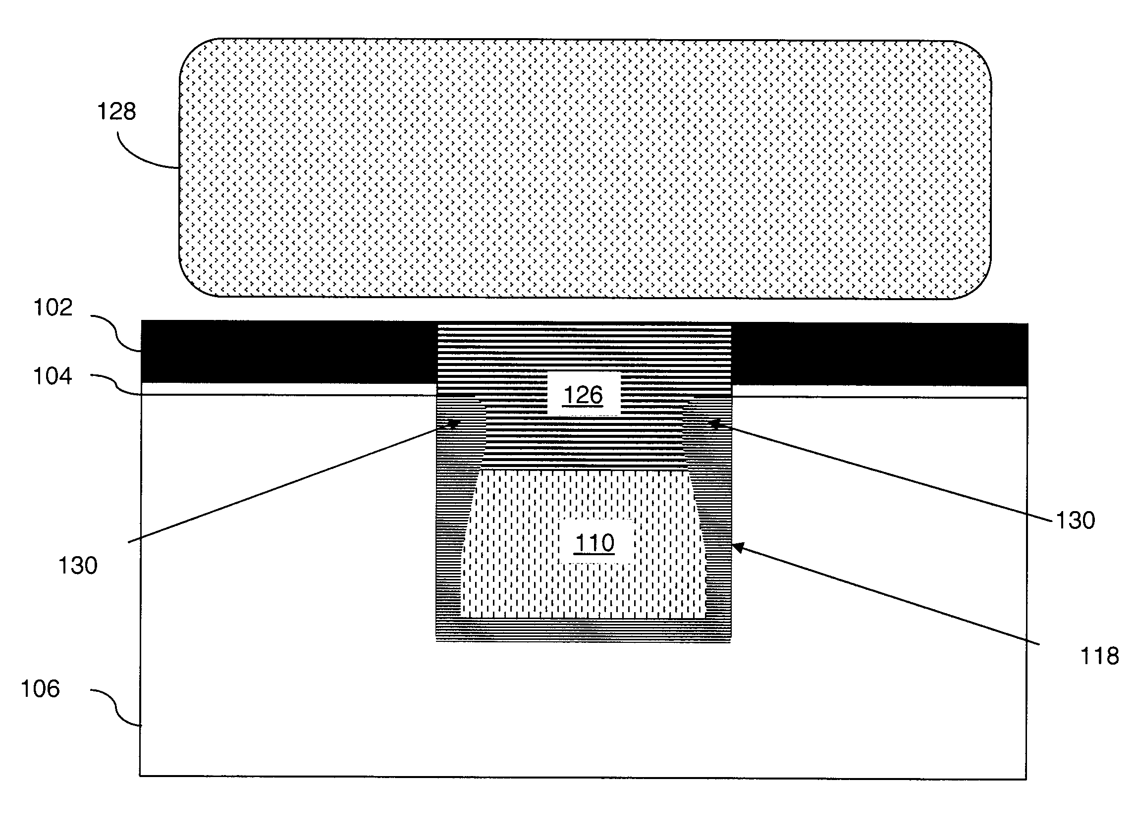
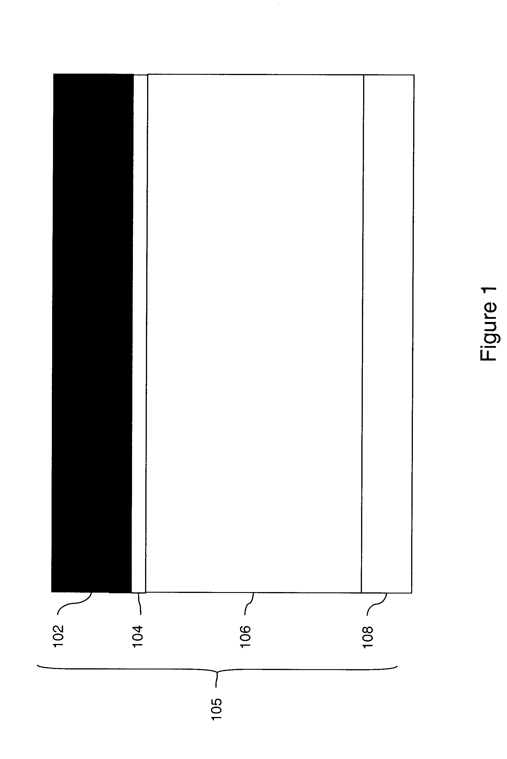
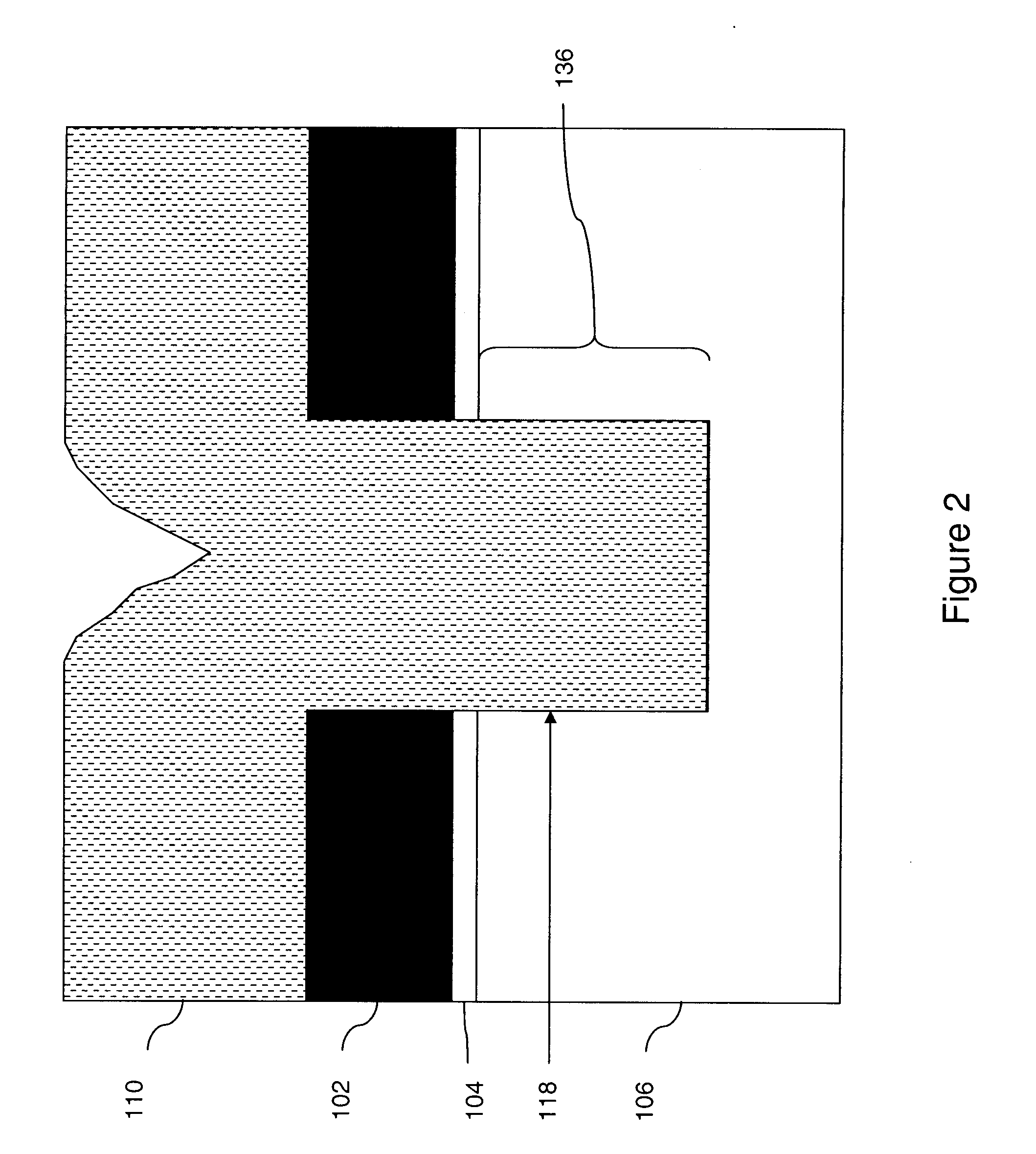
[0031] Referring to FIGS. 1-6 in combination, conventional shallow trench isolation (STI) structures are formed by etching trenches 136 of a depth of approximately 10-700 nm (shallower for SOI substrates and deeper for bu...


PUM


Abstract

A method and structure for an improved shallow trench isolation (STI) structure for a semiconductor device. The STI structure incorporates an oxynitride top layer of the STI fill. Optionally, the STI structure incorporates an oxynitride margin of the STI fill adjacent the silicon trench walls. A region of the oxynitride margin near the upper edges of the silicon trench walls includes oxynitride corners that are relatively thicker and contain a higher concentration of nitrogen as compared to the other regions of the oxynitride margin. The oxynitride features limit the STI fill height loss and also reduce the formation of divots in the STI fill below the level of the silicon substrate cause by hydrofluoric acid etching and other fabrication processes. Limiting STI fill height loss and the formation of divots improves the functions of the STI structure. The method of forming the STI structure is particularly compatible with standard semiconductor device fabrication processes, including chemical mechanical polishing (CMP), because the method incorporates the use of a pure silicon dioxide STI fill and plasma and thermal nitridation processes to form the oxynitride top layer and oxynitride margin, including the oxynitride corners, of the STI fill.

Description

FIELD OF THE INVENTION [0001] The present invention relates generally to a shallow trench isolation (STI) structure of a semiconductor device and method for forming an improved shallow trench isolation structure incorporating a pure silicon dioxide STI fill with an oxynitride top layer. DESCRIPTION OF THE RELATED ART [0002] Shallow Trench Isolation (STI) is used to electrically isolate semiconductor devices that make up an integrated circuit (IC). STI minimizes unwanted current leakage between the semiconductor devices, which can affect the performance of each semiconductor device. Generally, STI structures are formed by etching trenches into a silicon substrate. These trenches are then filled with an insulating dielectric STI fill such as, silicon dioxide (SiO2). The STI structures are formed early in the semiconductor-integrated circuit fabrication process flow. Therefore, the STI fill is exposed to many additional fabrication processes. These additional fabrication processes incl...

Claims


Application Information

Patent Timeline
Patent Type & Authority Applications(United States)
IPC IPC(8): H01L21/76
CPCH01L21/76224H01L21/76232H01L21/823481
Inventor BUEHRER, FREDCHOU, ANTHONY I.FURUKAWA, TOSHIHARUMO, RENEE T.
Owner IBM CORP
Why Eureka
Try Eureka