Frequency compensation scheme for a switching regulator using external zero

a switching regulator and compensation scheme technology, applied in the circuit field, can solve the problems of limiting the gain loss that can be achieved, affecting the operation of the output voltage,

Active Publication Date: 2007-01-30
MICREL
View PDF9 Cites 32 Cited by
  • Summary
  • Abstract
  • Description
  • Claims
  • Application Information

AI Technical Summary

Benefits of technology

[0028]The zero compensation scheme of the present invention has many advantages. First, the zero compensation scheme is simple for the user to implement as the user only needs to select a single component value—the zero capacitor—to realize effective Type III compensation. Second, by allowing the location of the second zero to be established through an external component, the compensation scheme allows for a wide range of inductor and capacitor values to be selected for the output filter circuit of the switching regulator. In general, the zero compensation scheme of the present invention provides a simplified approach for close loop compensation while providing flexibility for selecting inductance and capacitance values for the output filter circuit. The zero compensation scheme of the present invention can be effectively applied in switching voltage regulators and other closed loop feedback systems with multiple poles for introducing effective “zero” compensation and improving frequency stability.

Problems solved by technology

However, poles and zeros on the right half plane of a complex frequency plane are usually problematic and difficult to manipulate and is not addressed in the present application.
That is, at some point, the dynamic resistance of the gain stage will limit the gain loss capable of being achieved by the capacitor.
If the feedback control loop is not compensated, LC circuit 11 alone contributes an −180° phase shift to the system and loop instability results, causing the output voltage to oscillate.
When external compensation (off-chip) is used, it is often very difficult for users of the switching regulator to determine the optimal capacitance and resistance values for capacitors Cpole and Czero and resistors RIN and Rf in order to support a large range of output LC filter circuit values.
The transfer function to determine the capacitance and resistance values is often very complex.
When internal compensation (on-chip) is used, the range of output LC filter values is limited because the locations of the zero compensation are fixed by the on-chip compensation circuit.
The LC filter circuit must conform to the limited range of inductance and capacitance values or the feedback loop will become unstable.

Method used


Image

  • Frequency compensation scheme for a switching regulator using external zero
  • Frequency compensation scheme for a switching regulator using external zero
  • Frequency compensation scheme for a switching regulator using external zero

Examples


second embodiment

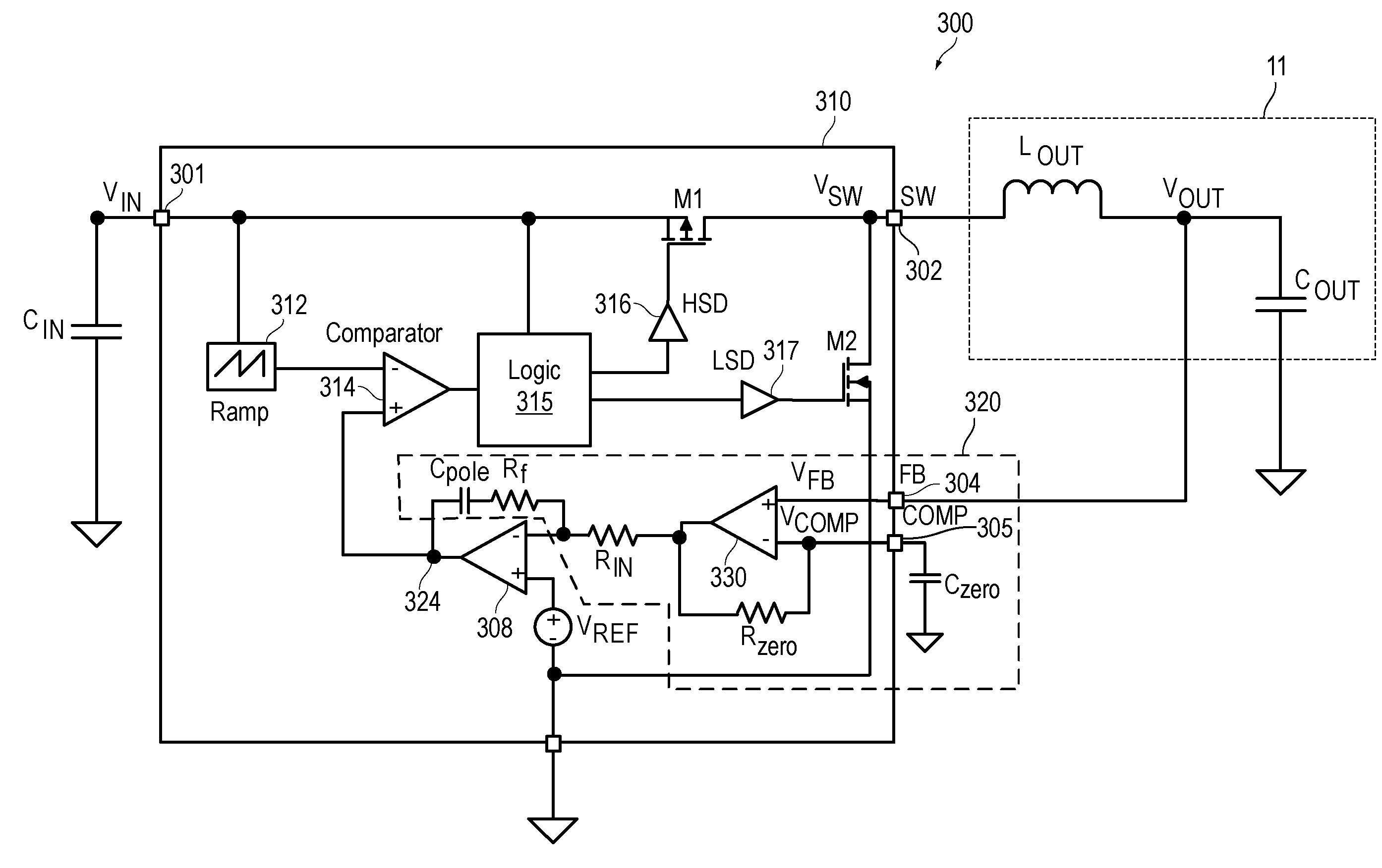
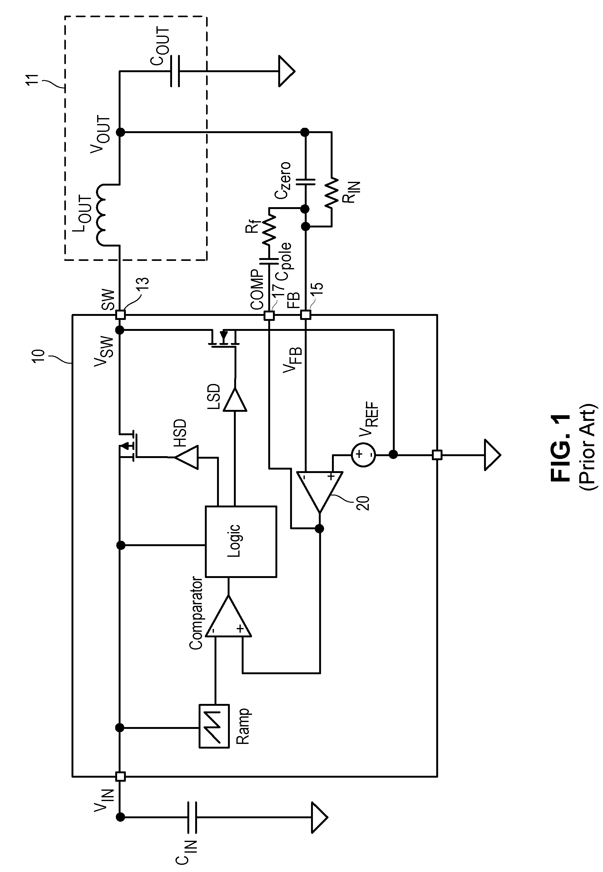
[0040]According to another aspect of the present invention, the zero compensation scheme of the present invention is applied in a switching regulator to implement type II compensation. FIG. 5 is a schematic diagram of a switching regulator including a monolithic switching regulator controller implementing the zero compensation scheme according to the present invention. In the embodiment shown in FIG. 5, the output capacitor COUT of switching regulator 500 is implemented using a high ESR capacitor, such as a tantalum or electrolytic capacitor. Because of the high ESR, the output capacitor COUT provides a zero itself to the feedback loop. Therefore, the switching regulator 500 requires only one additional zero. The zero compensation circuit 520 of the present invention can thus be utilized by leaving the COMP input terminal unconnected. That is, no external zero capacitor needs to be connected to the COMP input terminal of zero compensation circuit 520. Zero compensation circuit 520 p...

third embodiment

[0043]According to yet another aspect of the present invention, an external (off-chip) RC network can be coupled in parallel with the off-chip zero capacitor to modify the loop gain, in particular the mid-band gain, of the feedback loop of the switching regulator. FIG. 7 is a schematic diagram of a switching regulator including a monolithic switching regulator controller implementing the zero compensation scheme according to the present invention. Switching regulator 700 in FIG. 7 incorporates a zero compensation circuit in the same manner as switching regulator 300 of FIG. 3 and like elements in FIGS. 3 and 7 are given like reference numerals to simplify the discussion.

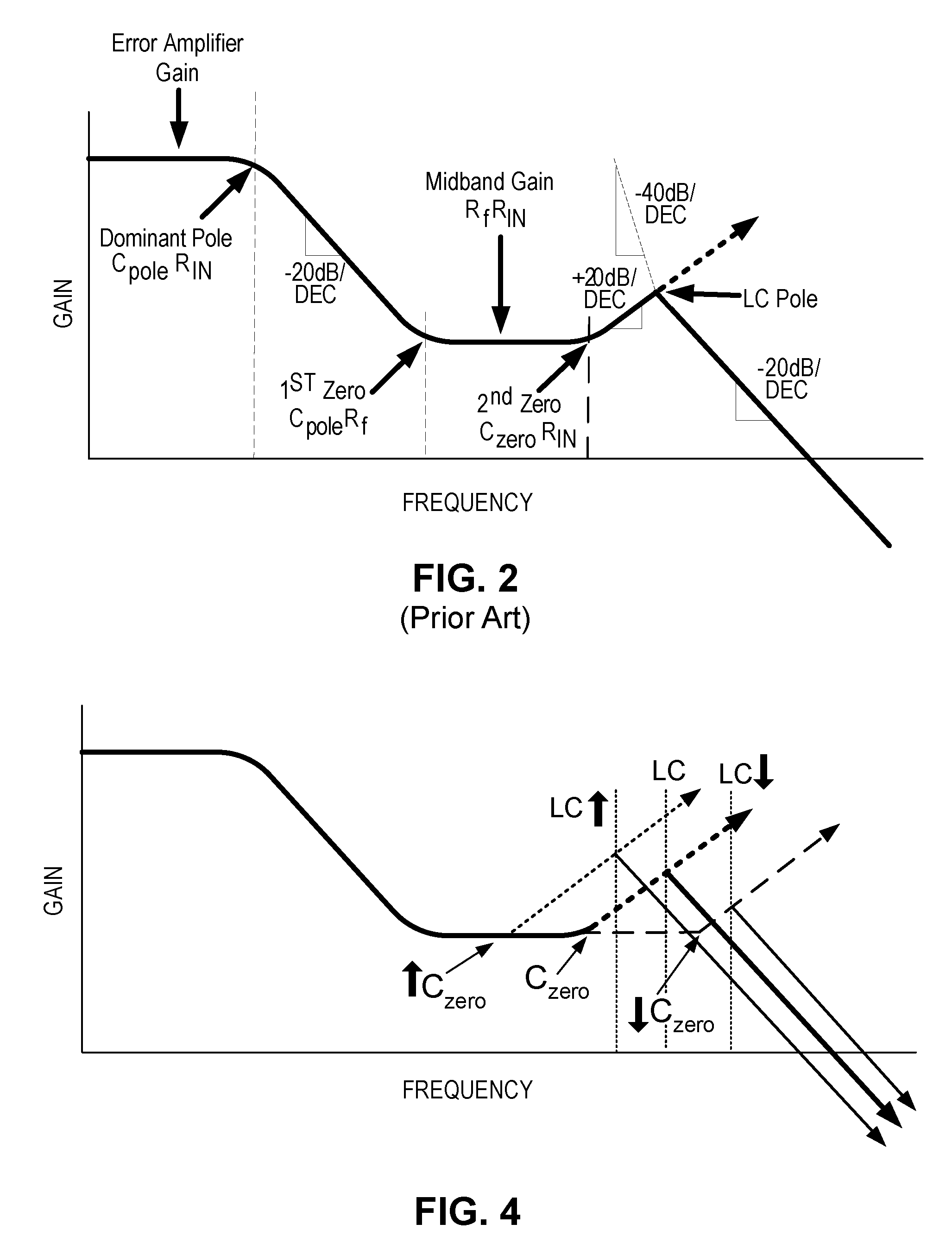
[0044]In switching regulator 700, the zero compensation circuit 720 includes a zero capacitor Czero coupled to the COMP input terminal 705 which connects to the inverting input terminal of amplifier 730. Zero capacitor Czero provides an external zero to the feedback loop. Furthermore, an RC network, including a seria...


PUM


Abstract

A compensation circuit in a monolithic switching regulator controller being incorporated in a closed loop feedback system of a switching regulator includes an amplifier configured in a unity gain feedback configuration with a first resistor and including a non-inverting input terminal receiving the feedback voltage and an inverting input terminal coupled to a first terminal of the switching regulator controller. The compensation circuit further includes a first capacitor and a third resistor connected in series between an input terminal and an output terminal of an error amplifier of the switching regulator controller. The first capacitor and the third resistor introduce a first zero in the closed loop feedback system. When a second capacitor is coupled to the first terminal of the switching regulator controller, a second zero is introduced in the closed loop feedback system. The second capacitor is an off-chip capacitor formed external to the monolithic switching regulator controller.

Description

FIELD OF THE INVENTION[0001]The invention relates to a circuit and method for providing zero compensation to a linear integrated circuit, in particular, to a circuit and method for providing compensation in a switching regulator feedback loop using an external zero.DESCRIPTION OF THE RELATED ART[0002]Closed loop negative feedback systems are commonly employed in linear integrated circuits. For instance, switching regulators use a feedback loop to monitor the output voltage in order to provide regulation. To ensure stability in any closed loop system, the Nyquist criterion must be met. The Nyquist criterion states that a closed loop system is stable if the phase shift around the loop is less than 180 degrees at unity gain. Typically, a compensation circuit is added to a feedback loop to modulate the phase shift of the feedback loop to obtain stability.[0003]The frequency response of a linear circuit can be characterized by the presence of “poles” and “zeros.” A “pole” is a mathematic...

Claims


Application Information

Patent Timeline
Patent Type & Authority Patents(United States)
IPC IPC(8): G05F1/10G05F1/652
CPCH02M3/156G05F1/62H02M3/1588G05F1/652
Inventor GALINSKI, MARTIN F.
Owner MICREL
Why Eureka
Try Eureka