Semiconductor thin film and method of manufacturing the same and semiconductor device and method of manufacturing the same

a technology of semiconductor devices and thin films, applied in the field of semiconductor devices, can solve the problems of inability to catch up to strict demands, inability to trace such trends, and inability to achieve the effect of overcoming the prior art, and achieving the effect of improving performance and reliability

Inactive Publication Date: 2007-02-06
SEMICON ENERGY LAB CO LTD
View PDF70 Cites 45 Cited by
  • Summary
  • Abstract
  • Description
  • Claims
  • Application Information

AI Technical Summary

Benefits of technology

[0015]It is another object of the invention to provide a new and improved semiconductor device capable of avoiding the problems faced with the prior art as well as the method for forming the same.
[0016]It is a still another object of the invention to provide a semiconductor integrated circuit device capable of offering enhanced performance and reliability without having to make use of single-crystalline semiconductor wafers.

Problems solved by technology

Unfortunately, the use of such amorphous films is encountered with a problem that where TFTs are required to exhibit higher operation speeds, amorphous films are incapable of trace such trend due to its inherently lowered mobility of charge carriers.
As the semiconductor manufacturers are commercially demanded to further improve the TFT speed endlessly, even the TFTs with such lateral-growth films as the active layer thereof will be unable to catch up the strict demands due to their inherent limitations as to improvements of the crystallinity.
Unfortunately, none of the prior art proposed are capable of overcoming this problem.
One reason for this is that the lateral growth silicon films do not come without accompanying a problem that reliability and productivity remain lowered due to the fact that the metallic element as used for acceleration of crystal growth might continue to reside within resultant silicon films, which disadvantageously serves to degrade the reproducibility.

Method used


Image

  • Semiconductor thin film and method of manufacturing the same and semiconductor device and method of manufacturing the same
  • Semiconductor thin film and method of manufacturing the same and semiconductor device and method of manufacturing the same
  • Semiconductor thin film and method of manufacturing the same and semiconductor device and method of manufacturing the same

Examples


Embodiment Construction

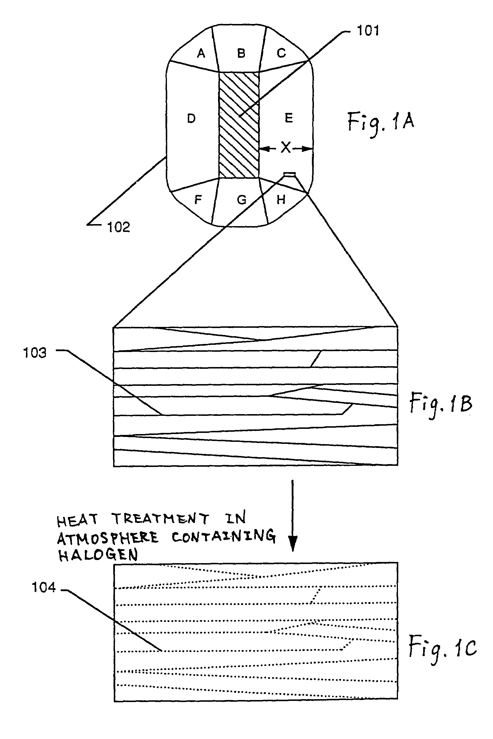
[0041]Before presentation of some illustrative embodiments of the present invention, the principal concept of fabrication of a “mono-domain” region which is a key to the invention will first be described with reference to FIGS. 1A to 1C, for purposes of convenience of understanding the gist of the invention.

[0042]See FIG. 1A. This is a diagrammatic depiction (not drawn to scale) of a plan view of a semiconductor thin film grown on a substrate surface. This thin film is made of a chosen semiconductor material, here, silicon. As shown, a chosen metallic element-doped region 101 is selectively formed on the substrate surface. With this region 101 being as a crystal seed, columnar or capillary crystals 102 are laterally grown in the direction essentially parallel to the crystal plane of the substrate surface.

[0043]The metallic element may act to facilitate or accelerate crystal growth or crystallization. The element may be iron (Fe), cobalt (Co), nickel (Ni), ruthenium (Ru), rhodium (Rh...


PUM

PropertyMeasurementUnit
surface heightaaaaaaaaaa
temperatureaaaaaaaaaa

Abstract

A thin film semiconductor transistor structure has a substrate with a dielectric surface, and an active layer made of a semiconductor thin film exhibiting a crystallinity as equivalent to the single-crystalline. To fabricate the transistor, the semiconductor thin film is formed on the substrate, which film includes a mixture of a plurality of crystals which may be columnar crystals and/or capillary crystal substantially parallel to the substrate. The resultant structure is then subject to thermal oxidation in a chosen atmosphere containing halogen, thereby removing away any metallic element as contained in the film. This may enable formation of a mono-domain region in which the individual columnar or capillary crystal is in contact with any adjacent crystals and which is capable of being substantially deemed to be a single-crystalline region without presence or inclusion of any crystal grain boundaries therein. This region is for use in forming the active layer of the transistor.

Description

CROSS-REFERENCE TO RELATED APPLICATIONS[0001]This application is a divisional application of U.S. application Ser. No. 08 / 805,952, filed Feb. 24, 1997 now U.S. Pat. No. 6,787,806, which claims the benefit of foreign priority applications filed in Japan as Ser. Nos. 08-061895 on Feb. 23, 1996 and 08-061896 on Feb. 23, 1996. This application claims priority to all of these applications, and all of these applications are incorporated by reference.BACKGROUND OF THE INVENTION[0002]1. Field of the Invention[0003]The present invention relates generally to semiconductor devices, and more particularly to semiconductor devices having a semiconductor thin film as its active layer and the manufacturing method thereof. The invention also relates to thin film semiconductor transistors with an active layer made of crystalline silicon films.[0004]2. Description of the Prior Art[0005]In the recent years semiconductor thin-film transistor (TFT) devices are becoming more widely used in the manufacture...

Claims


Application Information

Patent Timeline
Patent Type & Authority Patents(United States)
IPC IPC(8): H01L21/00G02B27/00G02B27/01H01L21/20H01L21/336H01L21/77H01L21/822H01L21/84H01L29/04H01L29/786
CPCG02B27/017H01L21/2022H01L29/045H01L27/1277H01L29/66757H01L29/78654H01L29/78675H01L29/665G02B2027/0138H01L21/8221H01L29/78621H01L21/02422H01L21/02488H01L21/02532H01L21/0242H01L21/02672H01L21/02381H01L29/786
Inventor YAMAZAKI, SHUNPEIKOYAMA, JUNMIYANAGA, AKIHARUFUKUNAGA, TAKESHI
Owner SEMICON ENERGY LAB CO LTD
Why Eureka
Try Eureka