Semiconductor display device

a technology of semiconductors and display devices, applied in the field of el display, can solve the problems of image having a desirable color cannot be displayed on the el display, the el material of the el layer is inferior to moisture, oxygen, light, etc., and achieve the effect of suppressing the reduction of the luminance of the el elemen

Inactive Publication Date: 2007-02-06
SEMICON ENERGY LAB CO LTD
View PDF18 Cites 39 Cited by
  • Summary
  • Abstract
  • Description
  • Claims
  • Application Information

AI Technical Summary

Benefits of technology

[0018]The present invention has been made in view of the above, and therefore has an object to provide an EL display capable of performing a clear and desirable color display by suppressing a reduction in luminance of an EL element even if an EL layer is deteriorated.
[0025]By adopting the above structure, the present invention has made it possible for the EL display to perform a clear and desirable color display by suppressing the reduction in luminance of the EL element even if the EL layer is deteriorated.
[0026]The EL display of the present invention may be of a color display system that employs a display EL element emitting white light, or a color display system that employs display EL elements corresponding to the colors RGB, respectively. In case of the color display system that employs the display EL elements corresponding to each of the colors RGB, it is preferable that the sensor pixels corresponding to each of the colors RGB are provided in the sensor portion. However, the present invention is not limited to the structure thereof. It may be a structure in which the sensor pixels, which correspond to either 1 or 2 colors of the RGB colors, are provided in the sensor portion. In particular, it is effective to provide the sensor pixel that corresponds to the color of which the deterioration of the EL layer is remarkable in the sensor portion to thereby display an image having a desirable color.
[0027]It is further preferable that the display EL element and the sensor EL element are formed at the same time under the same conditions. The deterioration rates of the EL layers of the display EL element and the sensor EL element can be made equivalent by adopting the above structure. Therefore, the luminance of the sensor EL element that will be detected by the light receiving diode becomes equivalent wraith the luminance of the display EL element, to thereby detect the change in the luminance of the display EL element more accurately. Thus, it becomes possible to revise the luminance of the display EL element to a desirable value.
[0028]Furthermore, when the sensor portion is formed simultaneously with the display portion on the substrate, as the manufacturing process of the El display, only the process of forming the light receiving diode has to be added to the manufacturing process in the case where the sensor portion is not provided. Therefore, there is no need to remarkably increase the number of manufacturing processes, thereby making it possible to suppress the number of manufacturing processes.

Problems solved by technology

The deterioration of the EL material of the EL layer has become a problem in the realization of the EL display, which leads to the reduction in the luminance of the EL element.
The EL material of the EL layer is inferior to moisture, oxygen, light, and heat, which are the factors that promote the deterioration of the EL layer.
Consequently, an image having a desirable color cannot be displayed on the EL display.

Method used


Image

  • Semiconductor display device
  • Semiconductor display device
  • Semiconductor display device

Examples


embodiment 1

[0136]An EL display of the present invention driven by an analog method is explained in Embodiment 1 using FIGS. 7 to 9.

[0137]Shown in FIG. 7 is a top view of an EL display, which is a portion of a semiconductor display device of the present invention. In Embodiment 1, an explanation will be made on an EL display for performing color display. However, the EL display of the present invention not only performs color display but may also perform monochrome display.

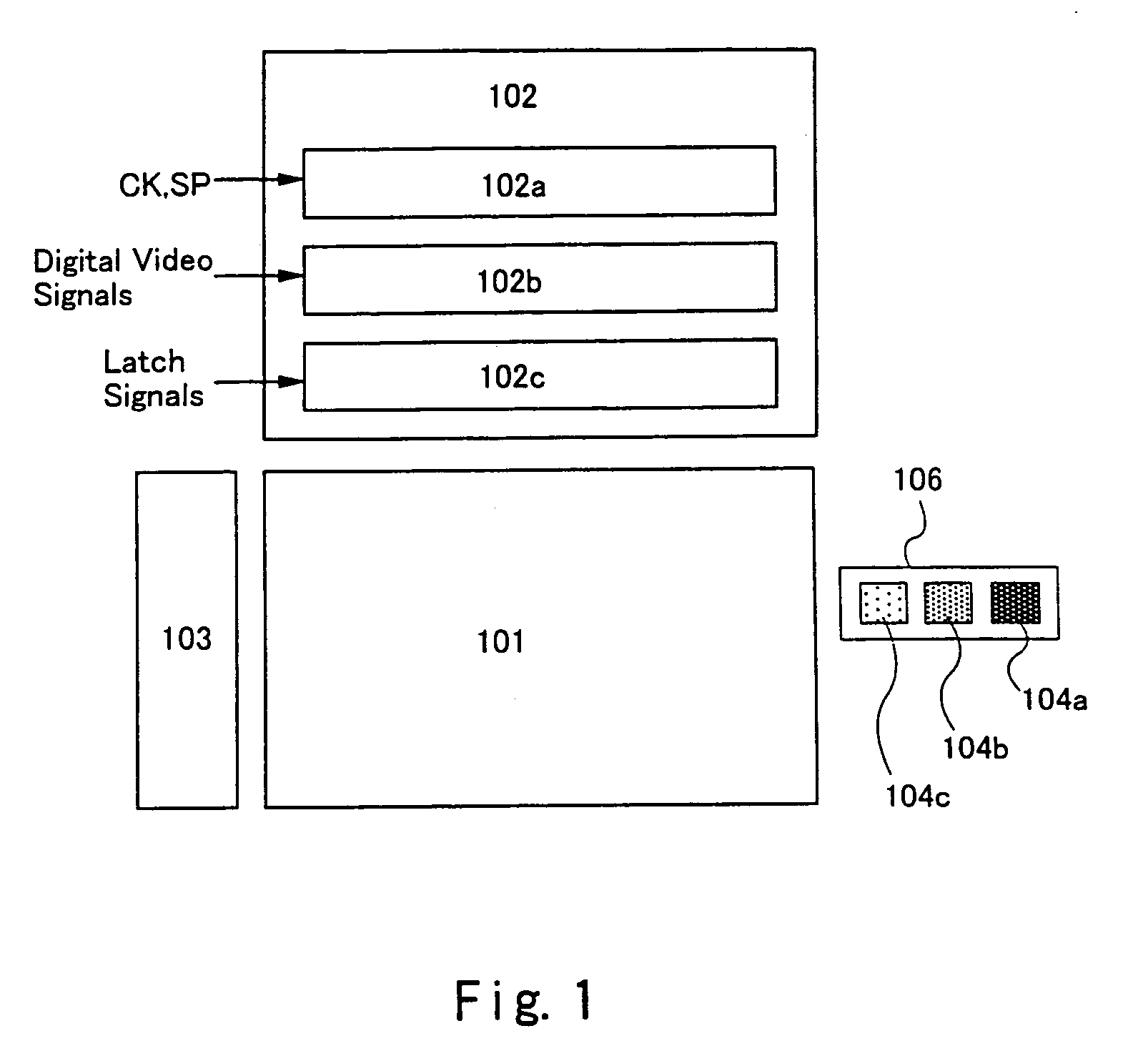
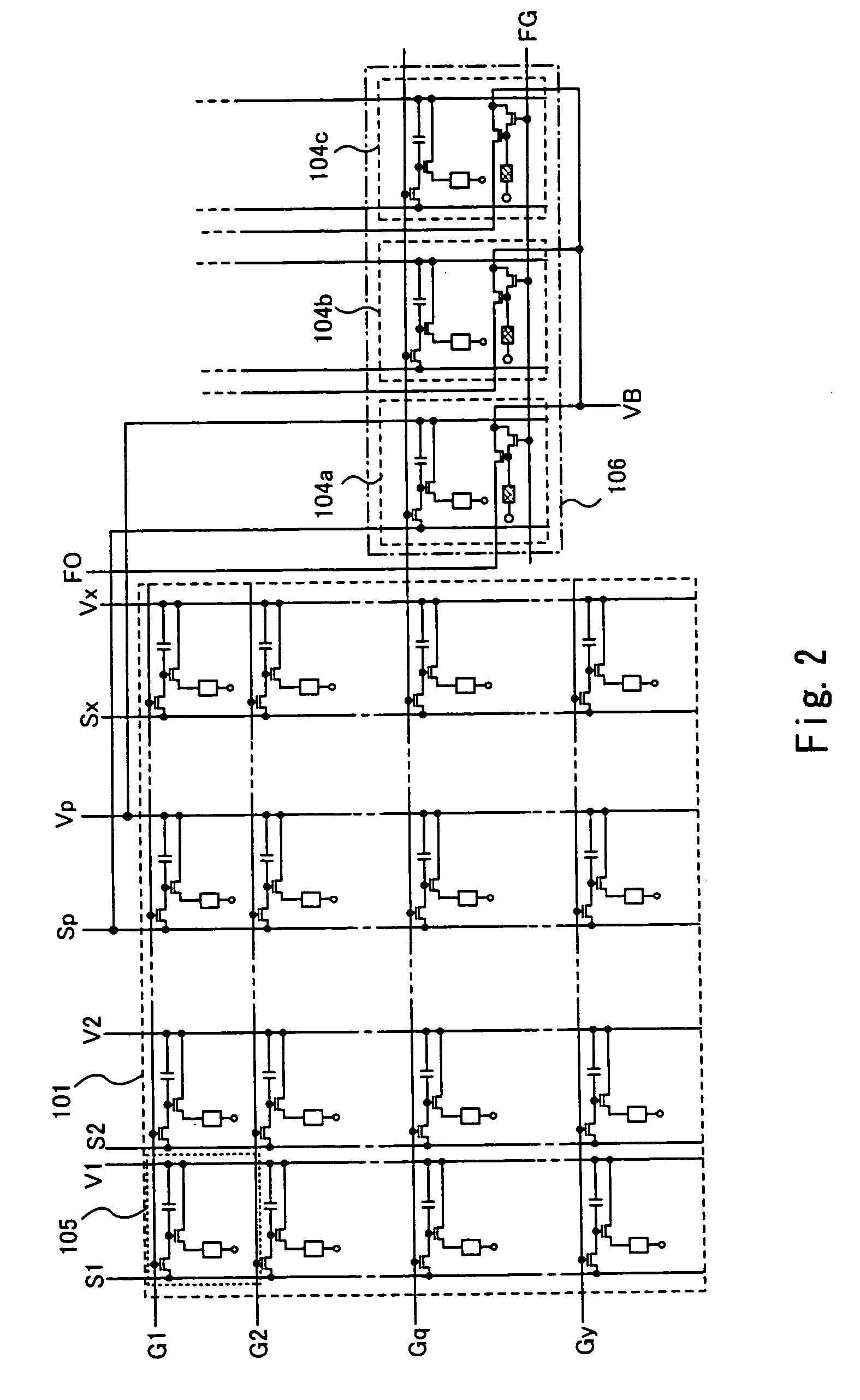
[0138]As shown in FIG. 7, there is provided a displays portion 301, a source signal line driver circuit 302, a gate signal line driver circuit 303, and a sensor portion 306. The source signal line driver circuit 302 is composed of a shift register 302a, a level shifter 302b, and a sampling circuit 302c.

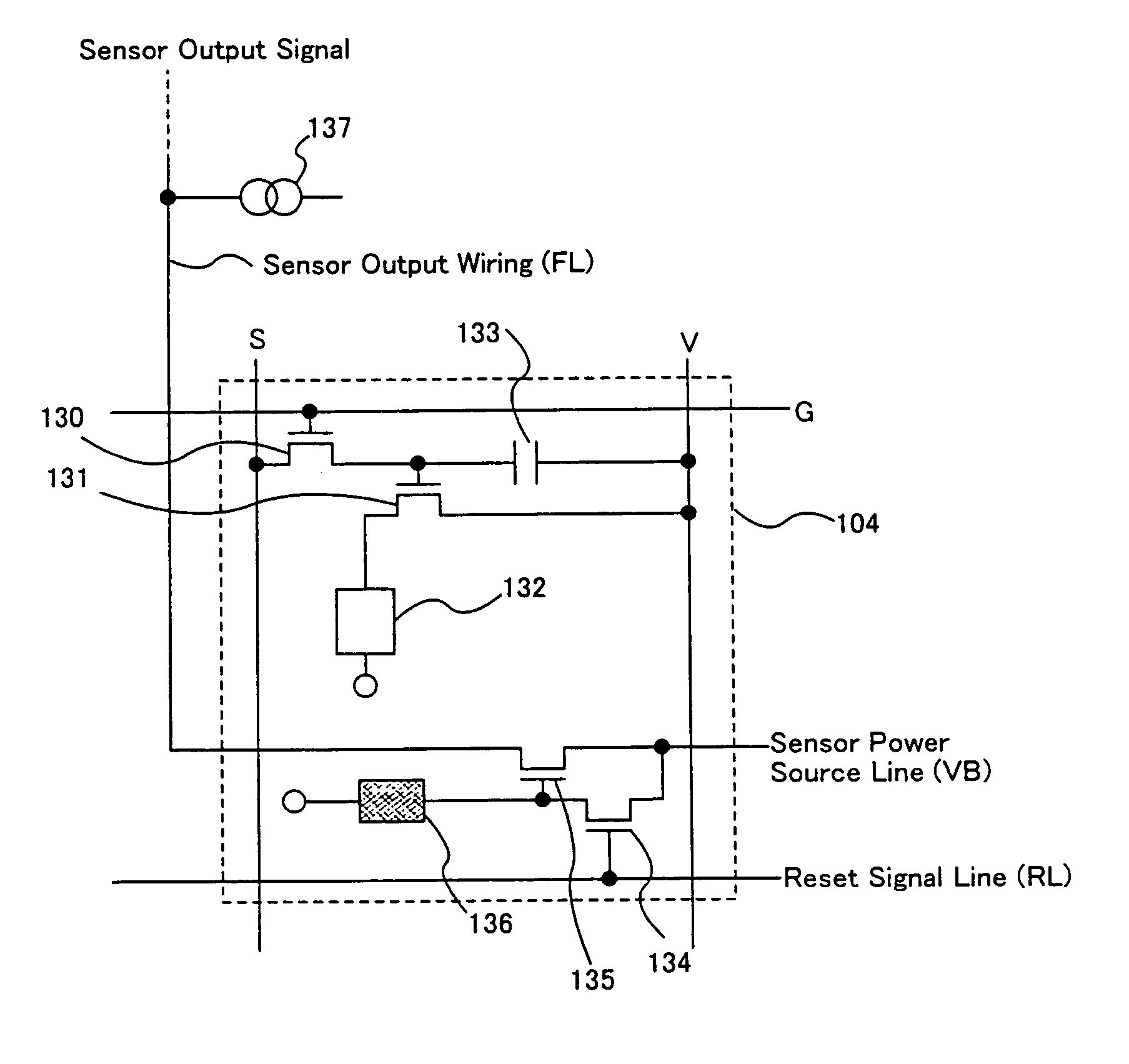
[0139]The sensor portion 306 has sensor pixels 304 (R sensor pixel 304a, G sensor pixel 304b, and B sensor pixel 304c) that correspond to the colors RGB, respectively. Note that an EL display of a color display system that emp...

embodiment 2

[0173]A method of manufacturing an EL display which uses the present invention is explained using FIGS. 10A to 13B. A method of manufacturing a TFT of a sensor portion is explained here, but it is also possible to similarly manufacture a TFT of a display portion.

[0174]First, as shown in FIG. 10A, a base film 501 is formed to a thickness of 300 nm on a glass substrate 500. A silicon oxynitride film is laminated as the base film 501 in Embodiment 2. At this point, it is appropriate to set the nitrogen concentration to between 10 and 25 wt % in the film contacting the glass substrate 500. In addition, it is effective that the base film 501 has a thermal radiation effect, and a DLC (diamond-like carbon) film may also be provided.

[0175]Next, an amorphous silicon film (not shown in the figure) is formed with a thickness of 50 nm on the base film 501 by a known deposition method. Note that it is not necessary to limit to the amorphous silicon film, and another film may be formed provided t...

embodiment 3

[0228]An example in which light emitted from an EL element is irradiated to the side of a substrate on which TFTs are formed is explained in Embodiment 2. Using FIG. 14, an example of irradiating light emitted from an EL element to the opposite side of the substrate on which TFTs are formed is explained in Embodiment 3.

[0229]Although a p-channel TFT was used for the EL driving TFT in Embodiment 2, an n-channel TFT was used for the EL driving TFT in this embodiment. Accordingly, the active later in the EL driving TFT was covered with a mask in a process for adding n-type impurity and the active layer in the EL driving TFT was not covered with the mask in the process for adding p-type impurity.

[0230]After forming a third interlayer insulating film 653, a contact hole for reaching a drain wiring 645 is formed in the third interlayer insulating film 653, a second interlayer insulating film 648, and a first passivation film 647. A pixel electrode 655 is then formed. Further, a contact ho...


PUM


Abstract

To provide a semiconductor display device capable of displaying an image having clarity and a desired color, even when the speed of deterioration of an EL layer is influenced by its environment. Display pixels and sensor pixels of an EL display each have an EL element, and the sensor pixels each have a diode. The luminance of the EL elements of each in the display pixels is controlled in accordance with the amount of electric current flowing in each of the diodes.

Description

CROSS-REFERENCE TO RELATED APPLICATIONS[0001]This application is a continuation application of U.S. application Ser. No. 10 / 195,521, filed Jul. 16, 2002, now U.S. Pat. No. 6,828,951, which is a divisional of U.S. application Ser. No. 09 / 753,708, filed Jan. 4, 2001, now U.S. Pat. No. 6,424,326, which claims the benefit of a foreign priority application filed in Japan as Serial No. 2000-002042 on Jan. 11, 2000. This application claims priority to each of these prior applications, and the disclosures of the prior applications are considered part of (and are incorporated by reference in) the disclosure of this application.BACKGROUND OF THE INVENTION[0002]1. Field of the Invention[0003]The present invention relates to an EL display that is formed by fabricating an EL (Electro Luminescence) element on a substrate. Particularly, the present invention relates to an active matrix type EL display that uses a semiconductor element (an element employing a semiconductor thin film), and furthermo...

Claims


Application Information

Patent Timeline
Patent Type & Authority Patents(United States)
IPC IPC(8): H01L31/20G09G3/20G09G3/32H01L21/77H01L21/84H01L27/12H01L27/146H01L27/32H01L29/786H05B44/00
CPCG09G3/3233G09G3/3258G09G3/3275H01L27/1214H01L27/3269H01L29/78624G09G3/2018H01L2251/5315G09G2300/0426G09G2300/0809G09G2300/0819G09G2300/0842G09G2300/0861G09G2310/027G09G2320/0285G09G2320/029G09G2320/043G09G2320/045G09G2330/021G09G2360/142G09G2360/145G09G2360/147G09G2360/148G09G2360/16H01L27/14678H01L27/3211H01L27/3246H01L27/3295H01L29/4908H01L51/5271G09G3/2022H10K59/35H10K59/122H10K59/13H10K50/856H10K2102/3026
Inventor YAMAZAKI, SHUNPEIKOYAMA, JUN
Owner SEMICON ENERGY LAB CO LTD
Why Eureka
Try Eureka