Receiver having an integrated clock phase detector
a clock phase detector and receiver technology, applied in the field of receivers having clock phase detectors, can solve the problems of large inherent noise of the output signal of the conventional clock phase detector, linear distortion of the reception signal, and additional noise components, and achieve the effect of minimising inherent nois
- Summary
- Abstract
- Description
- Claims
- Application Information
AI Technical Summary
Benefits of technology
Problems solved by technology
Method used
Image
Examples
third embodiment
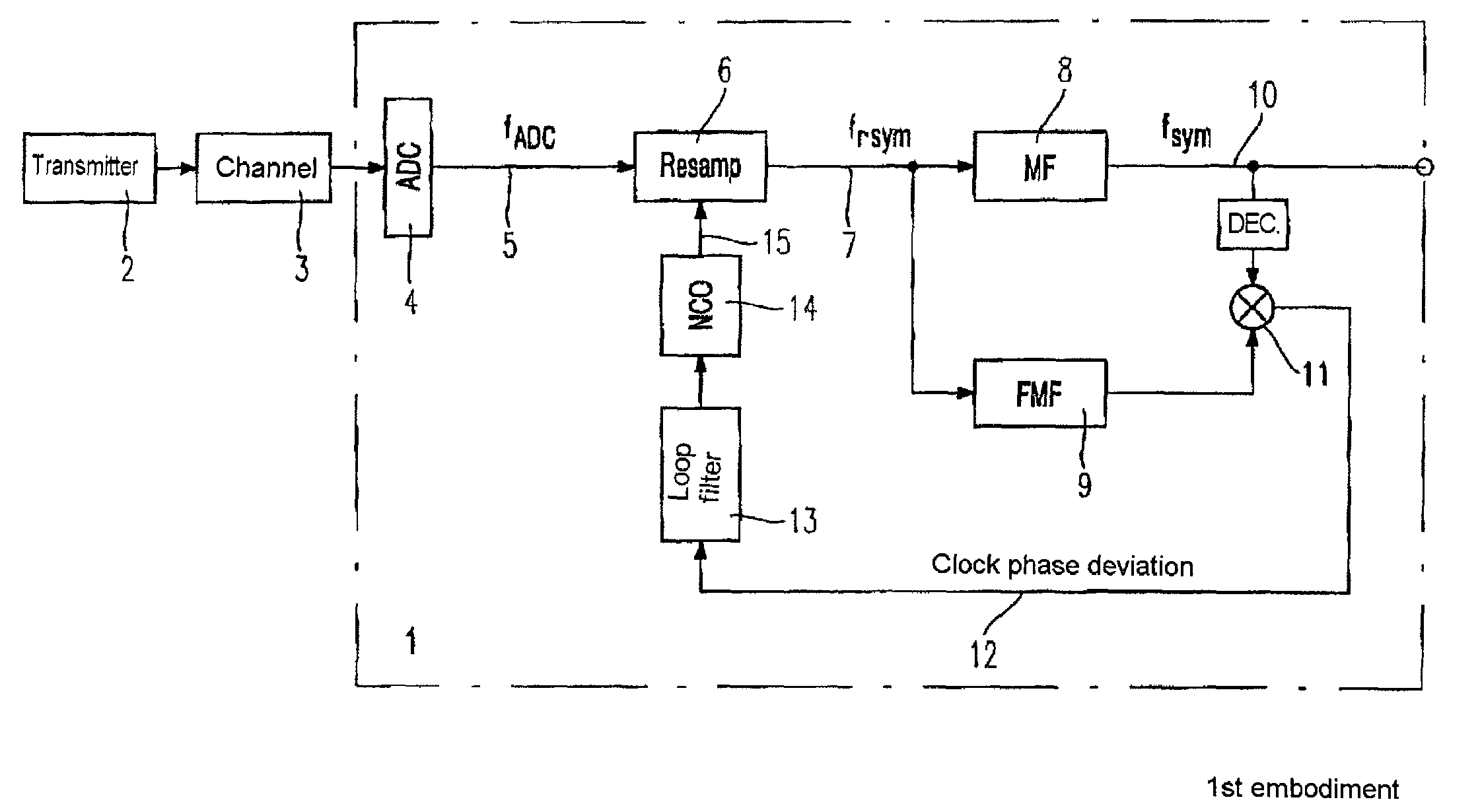
[0054]FIG. 6 shows the invention's receiver 1 with integrated clock phase detector.
[0055]In the embodiment illustrated in FIG. 6, the carrier frequency detection signal TF is formed from the filtered output signals of the matched filters 8 and the frequency matched filters 9 by two multipliers 11c, 11d and a further adder 17b. In this case, the multiplier 11d multiplies the in-phase signal component filtered by the matched filter 8a by the quadrature signal component filtered by the frequency matched filter 9b. In the same way, the multiplier 11d multiplies the quadrature phase signal component filtered by the matched filter 8b by the in-phase signal component filtered by the frequency matched filter 9a. The output signals of the two multipliers 11c, 11d are averaged by the adder 17b and output as carrier frequency detection signal TF via the line 18 to the digital loop filter 19.
second embodiment
[0056]Furthermore, the receiver 1 contains a clock phase loop 23, which is connected downstream of the two matched filters 8a, 8b. The clock phase detection signal TP is generated in the same way as in the second embodiment illustrated in FIG. 5. In the preferred embodiment of a QAM receiver as illustrated in FIG. 6, both the clock phase deviation detection signal TP and the carrier frequency deviation detection signal TF are generated from the output signals of the matched filters 8a, 8b and the frequency matched filters 9a, 9b. The receiver 1 illustrated in FIG. 6 therefore requires only a minimal number of filters in order to generate both the carrier frequency deviation detection signal TF and the clock phase deviation detection signal TP. The circuitry outlay for the multipliers 11a–11d and the two adders 17a, 17b is comparatively low.
fourth embodiment
[0057]FIG. 7 shows the receiver 1 according to the invention. Like the embodiment illustrated in FIG. 4, the embodiment of the receiver 1 as illustrated in FIG. 7 is a PAM receiver. In the PAM receiver 1 illustrated in FIG. 7, a clock phase filter 24 and a delay circuit 25 are connected downstream of the matched filter 8. The clock phase filter 24 and the delay circuit 25 are connected in parallel with one another, the output signals of the clock phase filter 24 and of the delay circuit 25 being multiplied by a multiplier 11 to form a clock phase deviation detection signal TP, which is output via a line 12 to a digital loop filter 13. The clock phase filter 24 is decimating in all of the embodiments, since the downstream multiplication is effected in the data symbol pattern.
[0058]The construction of the clock phase filter 24 contained in the receiver 1 is illustrated in FIG. 8. The clock phase filter 24 comprises two series-connected frequency matched filters 26, 27 and a Hilbert fi...
PUM
 Abstract
Description
Claims
Application Information


