Method for manufacturing a ceramic multilayer circuit board

a multi-layer circuit board and ceramic technology, applied in the direction of synthetic resin layered products, chemistry apparatus and processes, and the improvement of the adhesion of the metal to the insulation substrate, can solve the problems of the limit of wiring pitch and the achieve the effect of suppressing internal fracture of the ceramic green sheet, enhancing adhesion, and increasing the content of the resin binder in the conductive paste or ceramic green sh

Inactive Publication Date: 2007-03-06
PANASONIC CORP
View PDF30 Cites 5 Cited by
  • Summary
  • Abstract
  • Description
  • Claims
  • Application Information

AI Technical Summary

Benefits of technology

[0007]Content of the resin binder in the conductive paste or ceramic green sheet is increased. This will enhance adhesion between a conductive film and the ceramic green sheet when the conductive paste is filled in an intaglio and hot pressed on the ceramic green sheet, thereby removing transfer fa...

Problems solved by technology

However, in screen printing, 100 μm is the limit of wiring pitch (line width plus interwiring distance) in manufacturing.
However, as the solution of the adhesive layer contains high volatility solvent such as toluene and acetone, ceramic green sheet dissolves in the solution.
Also, even though an adhesive layer could have been f...

Method used


Image

  • Method for manufacturing a ceramic multilayer circuit board
  • Method for manufacturing a ceramic multilayer circuit board
  • Method for manufacturing a ceramic multilayer circuit board

Examples


first exemplary embodiment

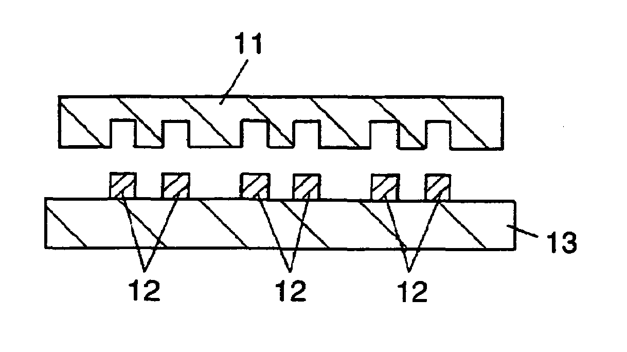
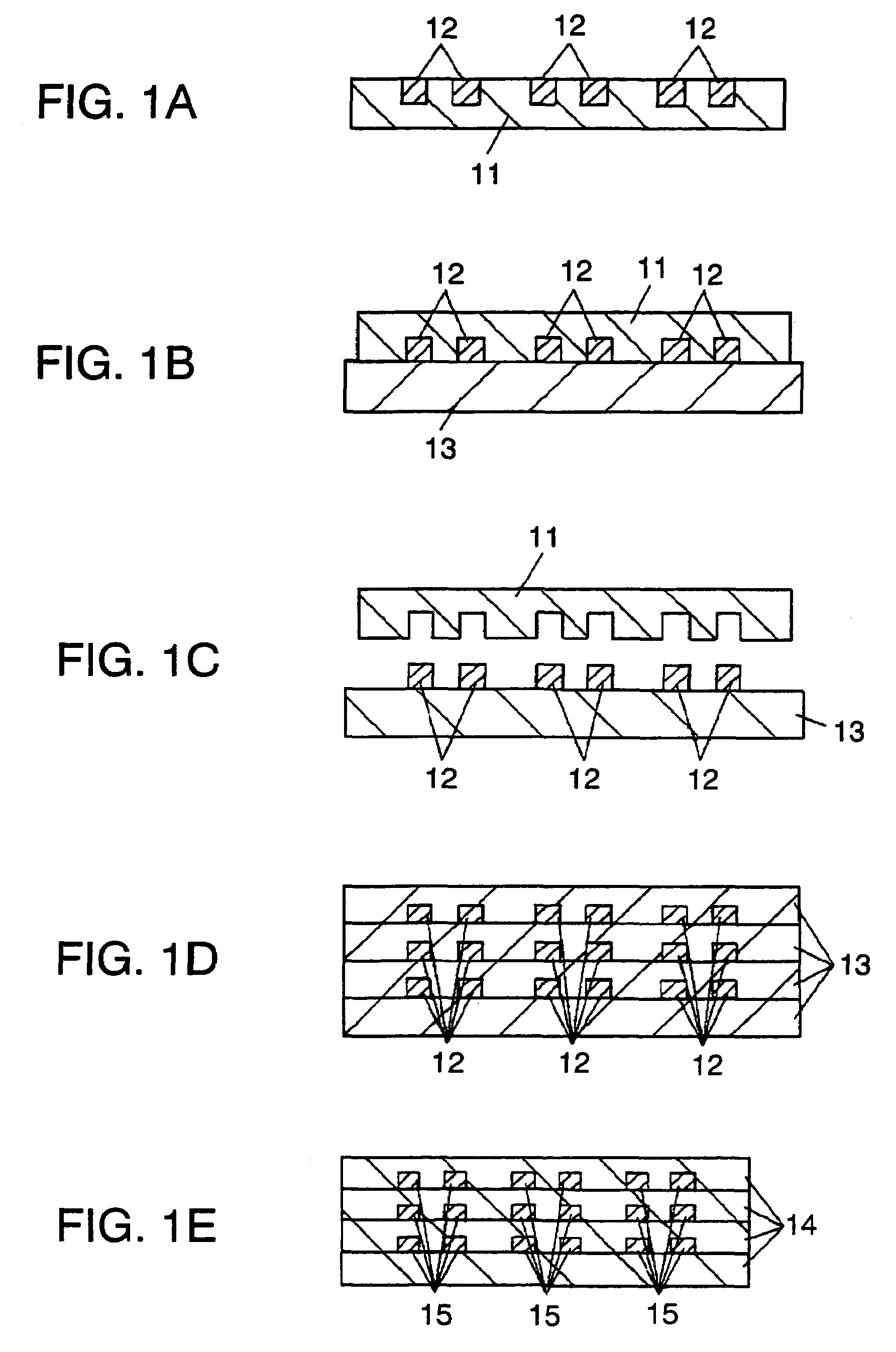
[0025]FIGS. 1A to 1E illustrate a method for manufacturing a ceramic circuit board by forming conductor patterns on a ceramic green sheet by thick-film intaglio transfer process.

[0026]In FIG. 1A, conductive paste 12 is filled with a ceramic blade or the like in intaglio 11 having grooves made by excimer laser, and dried. As the film for making the intaglio, heat resistant material such as polyimide or aramid is used after surface treatment in advance such as coating a mold-releasing agent for easy peeling while transferring.

[0027]Also, as conductive paste 12, silver-based paste is used which can be fired at 850° C. to 900° C. Intaglio 11 filled with conductive paste 12 is dried for 5 to 10 minutes at 100° C. to 150° C. After drying, the volume of conductive paste 12 filled in the grooves of intaglio 11 reduces due to evaporation of the solvent in the paste. Therefore, filling and drying of conductive paste 12 is repeated until recess of the dried surface of conductive paste 12 fille...

second exemplary embodiment

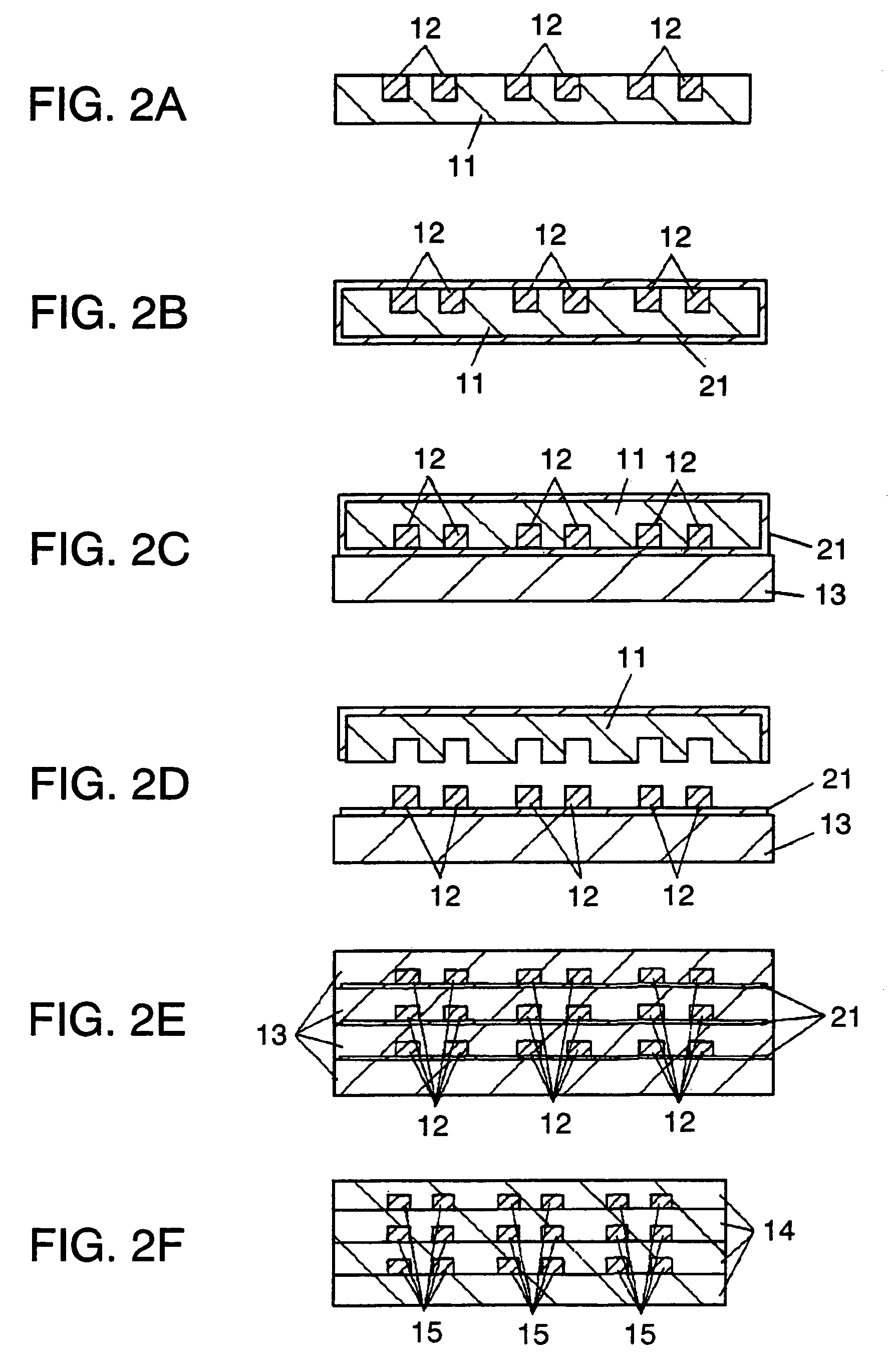
[0049]FIGS. 2A to 2F illustrate other method for manufacturing ceramic circuit board in which a conductor pattern is formed on a ceramic green sheet by thick-film intaglio transfer process. Elements similar to those in the first exemplary embodiment have the same reference numerals.

[0050]FIG. 2A illustrates the process of filling conductive paste 12 in intaglio 11. Details are similar to those in FIG. 1A in the first exemplary embodiment.

[0051]Next is the process of forming a uniform adhesive layer 21 with an adhesive agent solution on intaglio film 11 filled with conductive paste 12 by dipping or using roll coater as illustrated in FIG. 2B. The adhesive agent solution is prepared by dissolving thermoplastic resins such as butyral resin and acrylic resin into an organic solvent such as toluene, acetone, ethyl acetate, and methyl ethyl ketone.

[0052]Subsequently, as illustrated in FIG. 2C, a conductor pattern is formed on ceramic green sheet 13 by temporarily transferring conductive p...


PUM

PropertyMeasurementUnit
Temperatureaaaaaaaaaa

Abstract

By increasing the quantity of resin binder of at least one of conductive paste and ceramic green sheet, adhesion between conductive film and the ceramic green sheet is improved when an intaglio filled with the conductive paste is hot pressed on the ceramic green sheet. As a result, transfer failure at intaglio transfer is removed and internal fracture of the ceramic green sheet is suppressed. Also, by coating an adhesive layer on an intaglio filled with conductive paste, adhesion with ceramic green sheet is improved and transfer failure at intaglio transfer is suppressed.

Description

TECHNICAL FIELD[0001]The present invention relates to a method for manufacturing ceramic multilayer circuit board.BACKGROUND ART[0002]In recent years, ceramic multilayer circuit boards mainly employ low-temperature fired boards and are used as small components such as for personal computers and cellular phones. When manufacturing these ceramic multilayer boards, it is general practice to laminate ceramic green sheets. Screen printing method is generally employed in forming inner-layer wiring conductors while screen printing method, thin-film photolithography, or thick-film photolithography (for example, Fodel by DuPont) is employed in forming outer-layer wiring conductors.[0003]In extremely miniaturized electronic components to be used in devices such as cellular phones, printed circuit boards have built-in inductor elements (L), capacitor elements (C) or resistor elements (R). This has enabled development of circuit boards having an L-C-R combined circuit such as a filter. As L-C-R...

Claims


Application Information

Patent Timeline
IPC IPC(8): B32B37/06B44C1/165H05K3/20H05K3/46H05K1/03H05K3/38
CPCH05K3/207H05K1/0306H05K2203/0113H05K3/4611H05K3/4629H05K3/386
Inventor HASHIMOTO, AKIRAKATSUMATA, MASAAKI
Owner PANASONIC CORP
Why Eureka
Try Eureka