Semiconductor device

a technology of semiconductors and devices, applied in the direction of logic circuits, pulse techniques, radio frequency controlled devices, etc., can solve the problems of difficult to produce integrated circuit devices stable and uniform in quality, ensuring an operating margin for covering a process variation unavoidable in the lsi, and not readily implemented with conventional technology, etc., to achieve the effect of improving performance and ensuring stability

Inactive Publication Date: 2007-03-06
EXPL OF NEXT GENERATION
View PDF12 Cites 72 Cited by
  • Summary
  • Abstract
  • Description
  • Claims
  • Application Information

AI Technical Summary

Benefits of technology

[0021]As such, a semiconductor device capable of modulating an MOS transistor transistor's gain coefficient β by voltage in an analog manner can be readily produced with conventional processing technology and incorporated into any conventional LSIs configured of a CMOS circuit. As a result a circuit of a mechanism providing on-chip automatic adjustment of a device parameter to correct variation in characteristics can be mounted on any LSIs to implement a self-optimizing LSI, a self-adaptive LSI or other similar, completely new, active LSIs tolerating device characteristics varying to some extent. A limit can significantly be alleviated that is attributed to a variation in characteristics that is associated with device microfabrication, a variation in device characteristics that is associated with process variation or other similar unevenness in characteristics that has been a factor preventing a large-scale LSI from having enhanced performance.

Problems solved by technology

Nowadays, however, various physical limits manifest themselves in device microfabrication and it is becoming extremely difficult to produce integrated circuit devices which are stable and uniform in quality.
However, as LSIs have further various and complicated functions integrated therein, ensuring an operating margin for covering a process variation unavoidable in the LSI's production process has become an obstacle to further enhancing a large-scale LSI device in performance in future.
However, this has not readily been implemented with conventional technology.
This technique, however, is significantly inefficient in terms of precision in adjustment, and circuit scale.
The FIGS. 12 and 13 circuit configuration examples based on parallel connection are disadvantageous as precision with which characteristics can be adjusted and circuit scale have a trade-off relationship and enhanced precision of adjustment results in an increased circuit scale.
Furthermore, the FIGS. 14A–14C and 15A–15B circuit configuration examples based on series connection disadvantageously result in increased circuit scales and in addition provide an effective range of adjustment of characteristics that is limited by series interposition of a component of resistance indicating non-linear characteristics relative to an input signal.
As such, it hardly conforms with mounting a self-adjustment function for the purpose of pursuing high integration and enhancing the LSI in performance.

Method used


Image

  • Semiconductor device
  • Semiconductor device
  • Semiconductor device

Examples


first embodiment

[0035]Device Structure

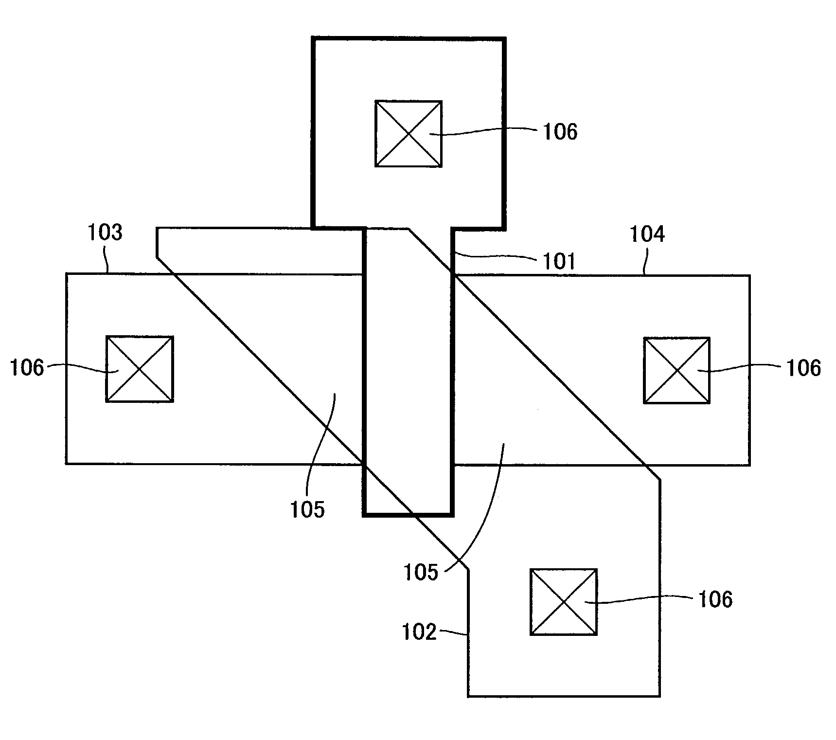
[0036]Initially in order to clarify a feature of a basic structure of the semiconductor device in a first embodiment FIG. 1 shows an exemplary configuration in layout regarding basic components of the device. In the first embodiment the semiconductor device is structurally characterized by additional introduction of a control gate having a fixed angle relative to a typical MOS gate.

[0037]FIG. 1 shows a typical MOS gate 101, a control gate 102, a source region 103, a drain region 104, a control channel region 105, and a contact region 106 electrically connected to a metal wire to extract an electrode.

[0038]In the first embodiment the semiconductor device is characterized in that control channel region 105 underlying control gate 102 substantially forms a triangle between typical MOS gate 101 and source 103 / drain 104, and control channel region 105 underlying control gate 102 and a channel region underlying MOS gate 101 together form a channel region substantiall...

second embodiment

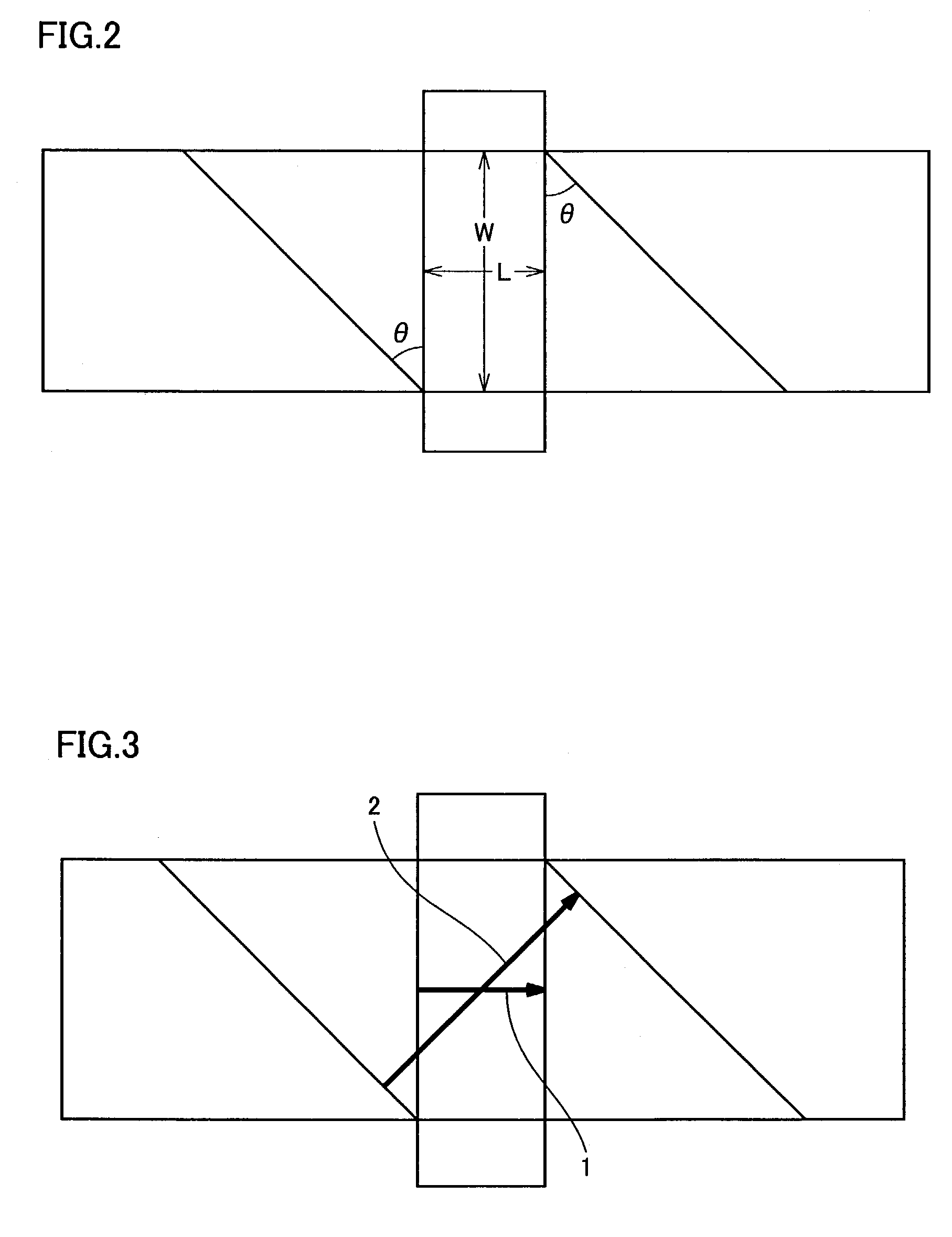
[0052]FIG. 8 shows a configuration of the semiconductor device of the present invention in a second embodiment. The second embodiment differs from the first embodiment in the geometry of control channel 105 underlying control gate 102. In this example, each control channel 105 is formed substantially in a trapezoid. Nonetheless, similar device characteristics can be achieved if each control channel 105 and the channel region underlying MOS gate 101 together form a channel region substantially in a parallelogram. Note, however, that the expressions (1)–(3) for approximation need to be modified slightly, as represented in expressions (4) and (5):

W′=cos θ*(W−(L+a+b)*tan θ)  (4)

L′=cos θ*(L+a+b+W*tan θ)  (5)

and β′ is in proportion to the following expression:

β′∝(W / L−(1+a / L+b / L)*tan θ) / (1+a / L+b / L+W / L*tan θ)  (6)

wherein a and b are each a length of a rectangular portion in each control channel of FIG. 8 that extends in the direction of the channel. The present embodiment indicates that a c...

third embodiment

[0053]FIG. 9 shows a configuration of the semiconductor device of the present invention in a third embodiment. The third embodiment is different from the first embodiment in that control gate 102 is formed by the same layer that forms MOS gate 101. If control gate 102 and MOS gate 101 are formed by a single gate layer the gates are electrically separated. Accordingly the gates are not allowed to overlap and, as shown in FIG. 9, they need to have a gap between control gate 102 and MOS gate 101 (so that they can be separated and processed).

[0054]Even in that case, the gap between control gate 102 and MOS gate 101 is provided in the same step that forms the source and drain, and the resistance is significantly small in value and this device configuration also exhibits characteristics which electrically do not differ from the first embodiment. Gain coefficient β modulated is approximated, as represented by expressions (4)–(6), wherein a and b represent a gap between control gate 102 and...


PUM


Abstract

In a semiconductor device an electric field is controlled in direction or angle relative to a gate, or a channel to adjust a gain coefficient of a transistor. In some embodiments, there are provided a first gate forming a channel region in a rectangle or a parallelogram, and a second gate forming a channel region substantially containing a triangle between the channel region formed by the first gate and each of a source region and a drain region. In some embodiments, there is included a channel region formed by the first gate that is sandwiched by the channel region formed by the second gate, all the channel regions together substantially forming a rectangle or a parallelogram. As such, a semiconductor device allowing a gain coefficient β of an MOS transistor to be modulated by voltage in an analog manner can readily be produced by conventional processing technology and incorporated into any conventional LSIs configured by a CMOS circuit.

Description

TECHNICAL FIELD[0001]The present invention relates generally to semiconductor devices allowing an MOS transistor's gain coefficient β to be modulated by voltage in an analog manner and more specifically to semiconductor devices incorporated into an LSI to allow each device to have its characteristics adjusted on-chip so that a scheme can be implemented to automatically correct a timing of an operation between incorporated functional circuits that is associated with increased sizes of LSIs, a variation in device characteristics that increases as the device is increasingly microfabricated, and the like so that the device is expected to contribute to high performance of the LSI based on optimization of individual chips.BACKGROUND ART[0002]Large scale integrated circuit (LSI) devices represented by semiconductor integrated circuits have steadily been developed in performance over 30 years since their invention mainly through device microfabrication. Nowadays, however, various physical l...

Claims


Application Information

Patent Timeline
Patent Type & Authority Patents(United States)
IPC IPC(8): H01L29/76H01L21/8234H01L27/088H01L29/423H01L29/78H03K19/00
CPCH01L29/7831H01L29/4238
Inventor ARIMA, YUTAKA
Owner EXPL OF NEXT GENERATION
Why Eureka
Try Eureka