Distributed power MOSFET

a technology of distributed power and mosfet, which is applied in the field of semiconductor devices, can solve the problems of reducing the area available for other circuitry in the device b>2, and achieve the effects of reducing the area of the total power transistor device, facilitating improved space utilization, and reducing device siz

Inactive Publication Date: 2007-03-06
TEXAS INSTR INC
View PDF8 Cites 3 Cited by
  • Summary
  • Abstract
  • Description
  • Claims
  • Application Information

AI Technical Summary

Benefits of technology

[0011]According to one aspect of the invention, transistors are provided, in which the transistor is segmented into two or more transistor segments having segment sizes or areas determined according to a safe operating area (SOA) specification for the device, which are then coupled to form a segmented transistor device. The transistor segments themselves may be further partitioned, such as comprising two or more partitioned source and drain diffusion areas or cells in the wafer. This aspect of the invention may be employed in association with LDMOS and other MOS type devices to facilitate improved space utilization and / or reduced device sizes, while achieving performance and safe operating specifications. In this regard, the various aspects of the invention may be practiced to effectively reduce the total power transistor device areas below that required for equivalent unitary (e.g., non-segmented) devices. In other implementations, the invention may be employed to provide transistors of the same or similar size or area, which have higher power handling capabilities than similarly sized non-segmented transistors.
[0012]In another aspect of the invention, the transistor segments are spaced from one another according to a pulse time specification for the device. This may be employed, for example, to provide thermal diffusion distance in the substrate between adjacent segments, through which heat is removed from the device to reduce the likelihood of thermal damage or failure during operation. In still another aspect, other electrical devices may be formed in the spaces between the power transistor segments, in order to better utilize the total area of the device die. For example, in a solenoid driver device, logic and / or low power analog circuitry such as transistors, memory cells, resistors, capacitors, diodes, or the like, may be located between the spaced power transistor segments in the substrate. Thus, in addition to facilitating reduction in the total transistor area, the invention facilitates improved space utilization (e.g., higher device density) throughout the device, by which more circuitry may be provided in a given die area, and / or by which die areas may be reduced.

Problems solved by technology

Thus, designers are often forced to oversize the transistors 8 beyond the area required to meet Rdson specifications, in order to achieve SOA specifications, thereby reducing the area available for other circuitry in the device 2.

Method used


Image

  • Distributed power MOSFET
  • Distributed power MOSFET
  • Distributed power MOSFET

Examples


Embodiment Construction

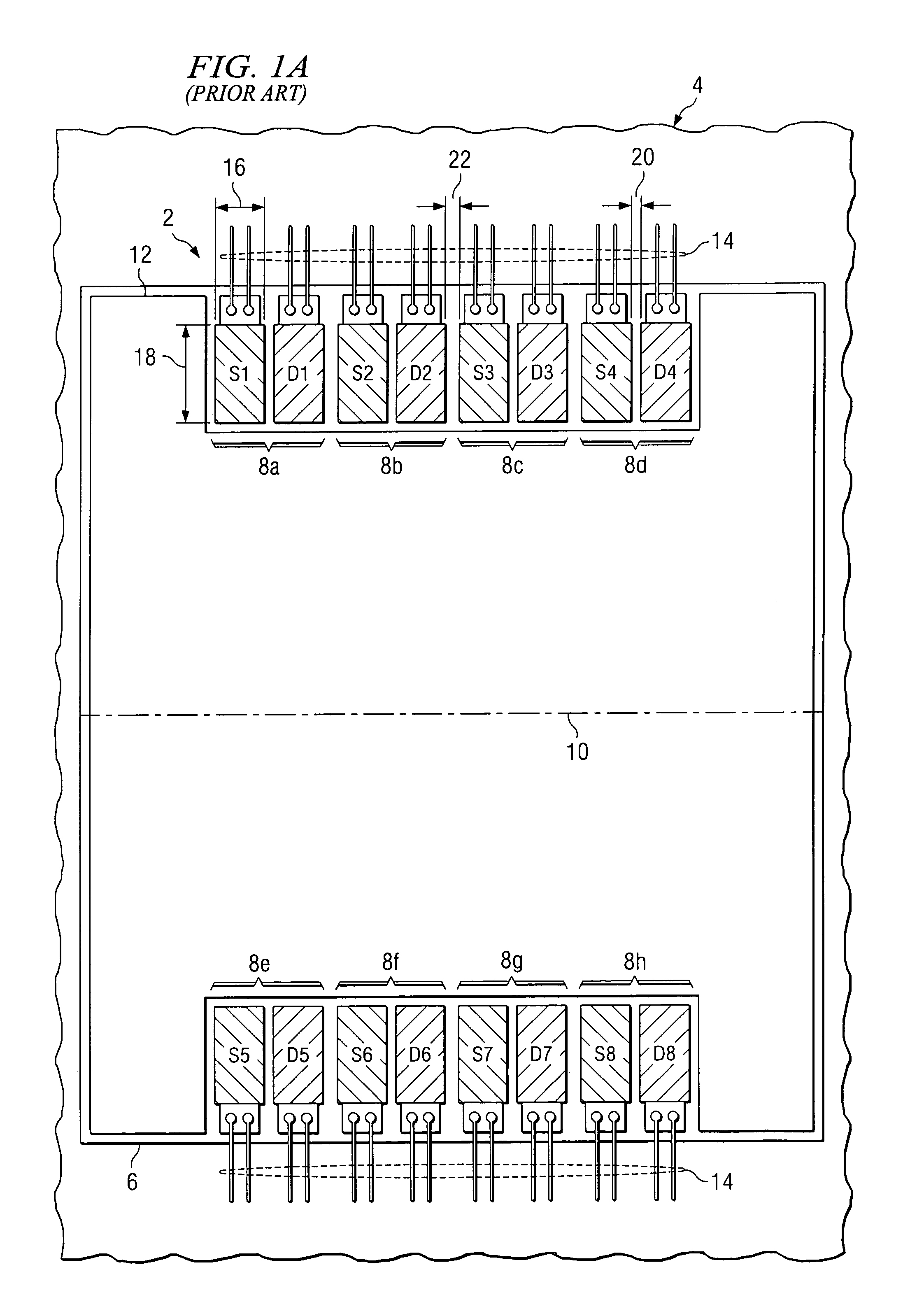
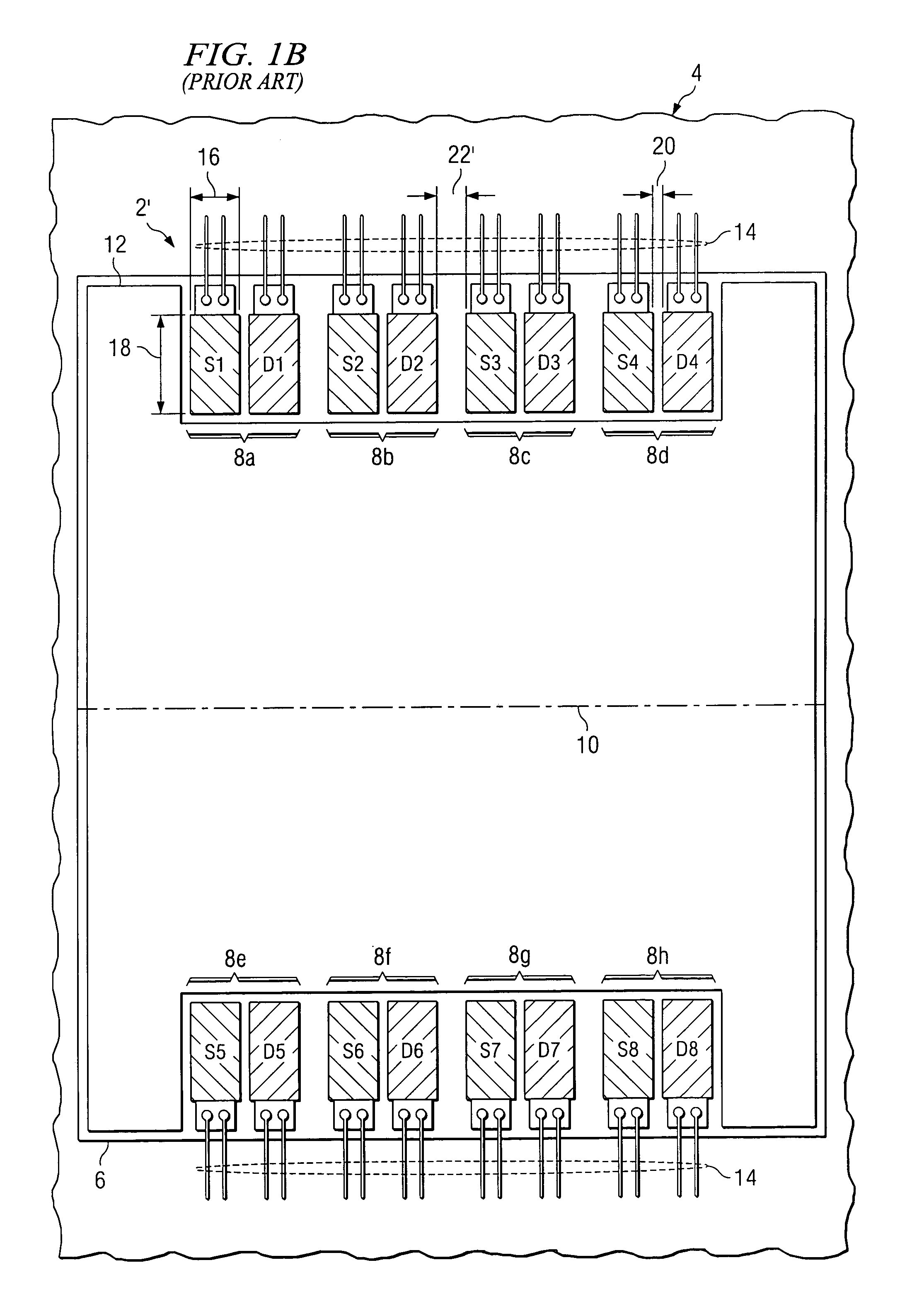
[0030]The present invention will now be described with reference to the attached drawings, wherein like reference numerals are used to refer to like elements throughout. Several implementations of the various aspects of the invention are hereinafter illustrated and described in the context of LDMOS devices in solenoid driver circuits. However, it will be appreciated that the invention is not limited to such devices, and that the various aspects of the invention may be carried out in conjunction with any type of power semiconductor device and any type of transistor.

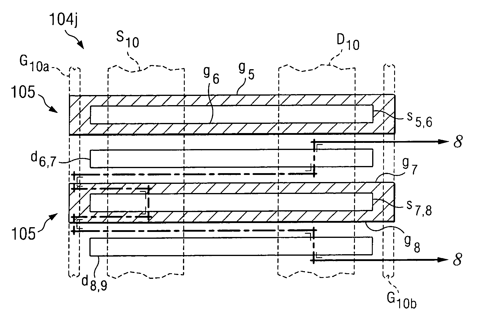
[0031]Referring to FIGS. 2A–6, one example of a segmented LDMOS power transistor 100 is illustrated in a driver device 102 in accordance with the invention. The invention contemplates segmented transistor devices having any integer number N transistor segments, one some or none of which may be individually partitioned to comprise multiple source and drain diffusion regions, ‘si’ and ‘di’, and polysilicon gate structures gi...


PUM


Abstract

Segmented power transistors and fabrication methods are disclosed in which transistor segments are spaced from one another to facilitate thermal diffusion, and in which other electrical devices can be formed in the spaces between transistor segments.

Description

[0001]This is a divisional application of Ser. No. 10 / 264,038 filed Oct. 3, 2002, now U.S. Pat. No. 6,815,276.FIELD OF INVENTION[0002]The present invention relates generally to semiconductor devices and more particularly to segmented power MOSFET devices and methods for making the same.BACKGROUND OF THE INVENTION[0003]Many modern power semiconductor devices are fabricated using lateral double-diffused metal-oxide-semiconductor (LDMOS) transistors, sometimes referred to as lateral DMOS devices. LDMOS transistors are asymmetrical MOSFET devices, wherein a p-type channel region is diffused in a low-doped n-type drain region. Low doping on the drain side provides a large depletion layer with high blocking voltage. Moreover, the channel region diffusion can be defined with the same mask as the source region, resulting in a short channel with high current handling capabilities. Also, the relatively deep p-type diffusion causes a large radius of curvature, thereby mitigating edge effects a...

Claims


Application Information

Patent Timeline
Patent Type & Authority Patents(United States)
IPC IPC(8): H01L29/78H01L23/482H01L29/06H01L29/417H01L29/423
CPCH01L29/7801H01L23/4824H01L29/0696H01L29/41758H01L29/4238H01L2924/0002H01L2924/00H01L29/7816
Inventor HOWER, PHILIP L.LIN, JOHNPENDHARKAR, SAMEER P.MERCHANT, STEVEN L.
Owner TEXAS INSTR INC
Why Eureka
Try Eureka