Advanced illumination system for use in microlithography

a technology of illumination system and microlithography, applied in the field of microlithography, to achieve the effect of simple optics

Inactive Publication Date: 2007-03-06
ASML HLDG NV
View PDF37 Cites 19 Cited by
  • Summary
  • Abstract
  • Description
  • Claims
  • Application Information

AI Technical Summary

Benefits of technology

[0011]One advantage of the present invention is being able to provide a microlithographic system with continuously adjustable partial coherence and discretely adjustable field size.
[0012]Another advantage of the present invention is being able to provide a microlithographic system where both partial coherence and field size can vary continuously.
[0013]Another advantage of the present invention is being able to provide a microlithographic system that can achieve the above objectives with the use of simple optics.

Problems solved by technology

However, a particular problem arises in the field of microlithography, where different features that are required to be formed on the semiconductor substrate require variable partial coherence on the part of the exposure optics.

Method used


Image

  • Advanced illumination system for use in microlithography
  • Advanced illumination system for use in microlithography
  • Advanced illumination system for use in microlithography

Examples


Embodiment Construction

[0028]Reference will now be made in detail to the preferred embodiments of the present invention, examples of which are illustrated in the accompanying drawings.

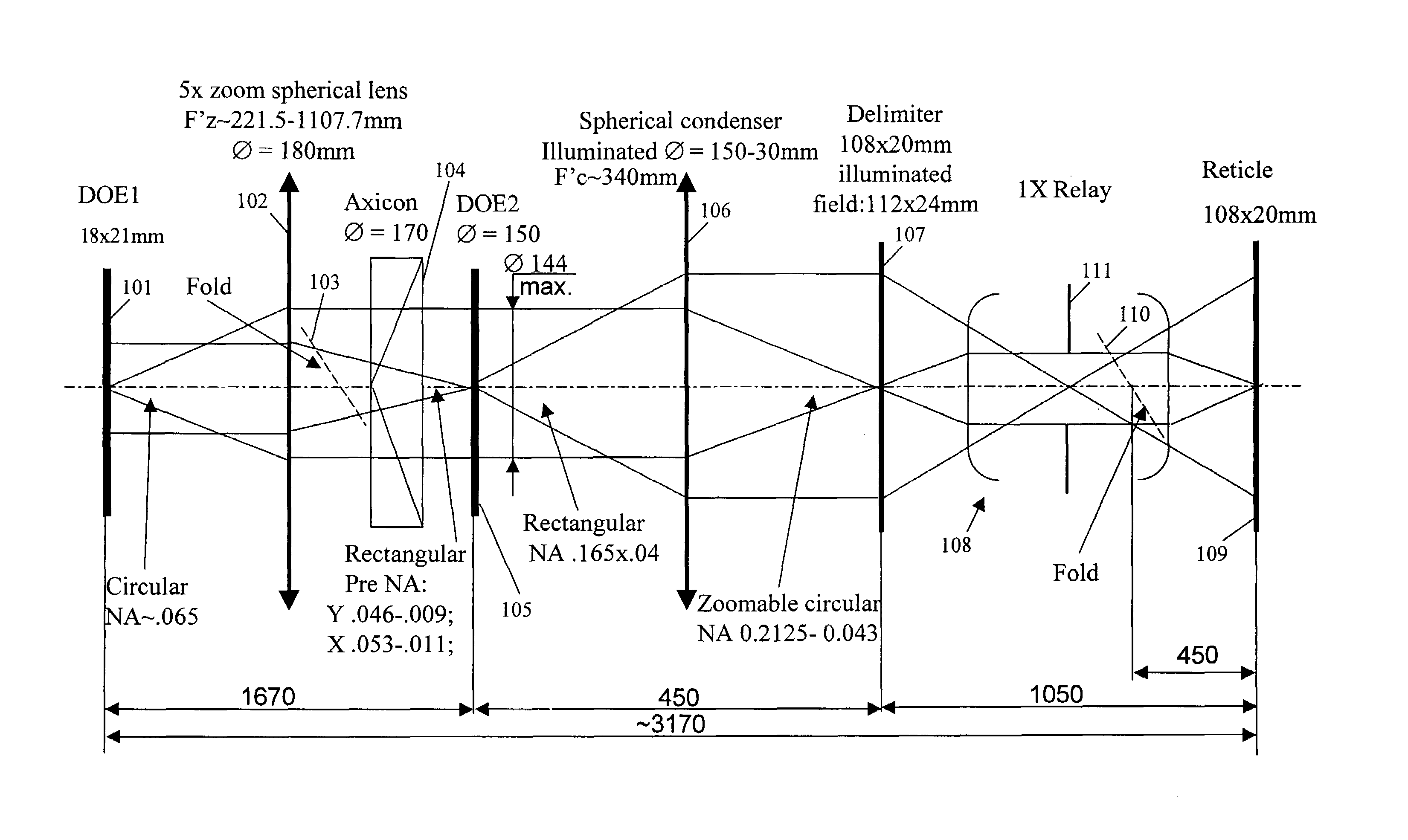
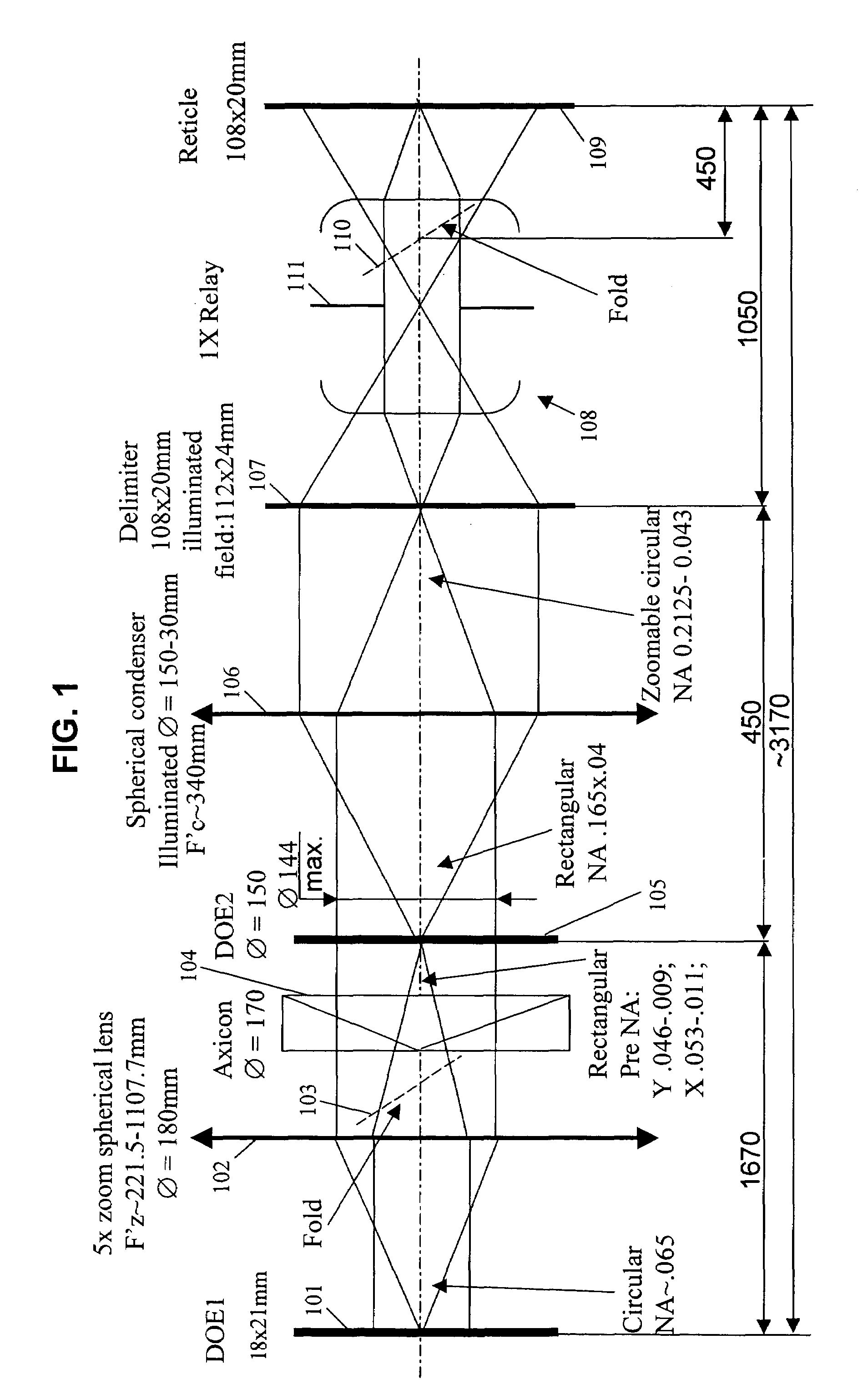
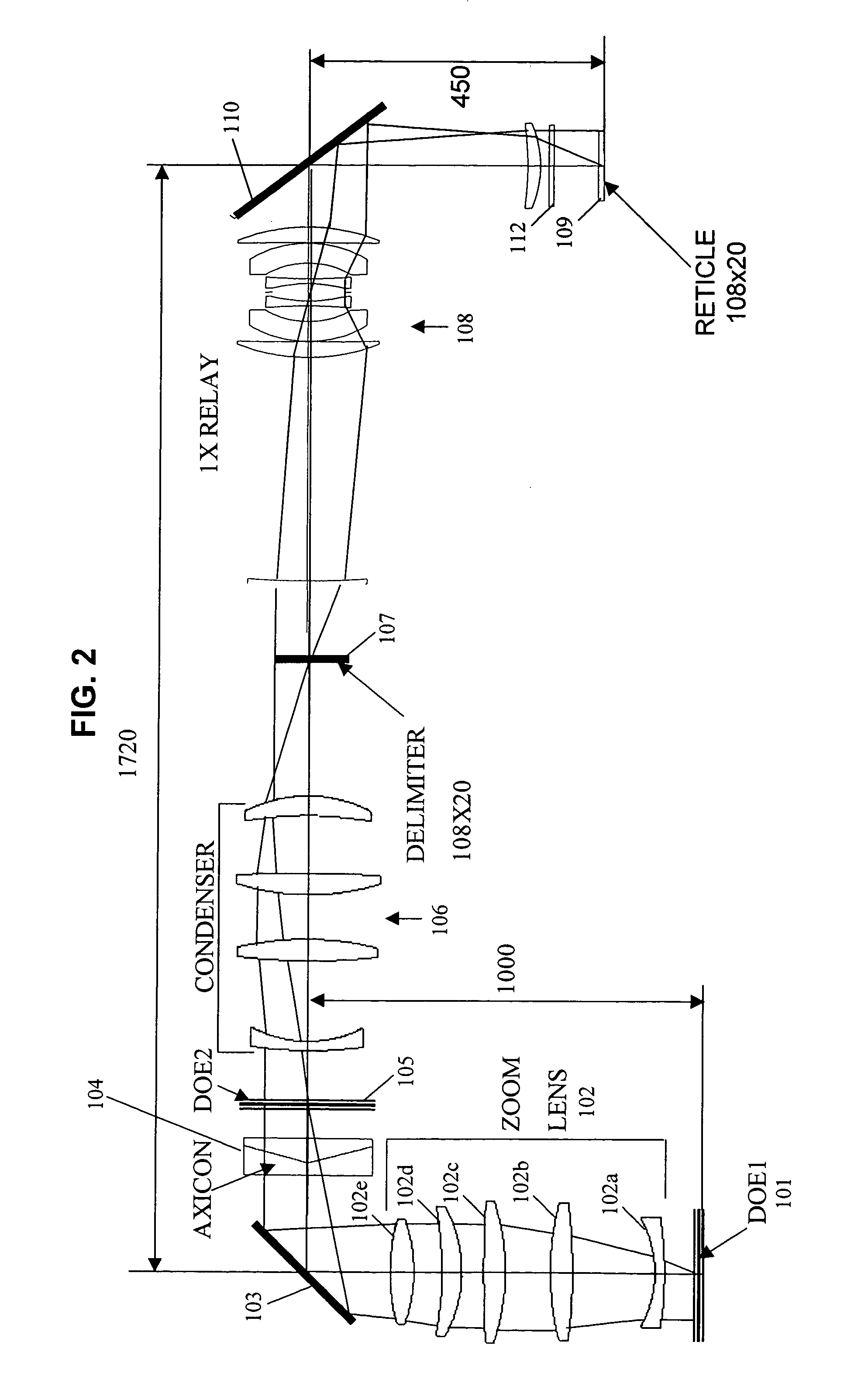
[0029]In recent years, photolithography used in semiconductor device fabrication has been moving to gradually shorter wavelengths, as device features shrink in size. With feature sizes shrinking to sub-micron- and sub-0.1μ range, semiconductor manufacturers have had to shift to the use of ultraviolet light, and in some cases to soft X-ray lithography (or deep UV). For example, excimer lasers, which emit light in the 248, 193 and 157 nm range, are increasingly used in semiconductor device fabrication. The illumination source in modem microlithographic equipment, as noted above, is typically a visible light laser, an excimer laser, or possibly a, soft X-ray source. (The terms “light” and “illumination” will be used interchangeably hereafter to refer to any electromagnetic radiation used for photoresist exposure.) The use of th...


PUM

PropertyMeasurementUnit
diameteraaaaaaaaaa
diameteraaaaaaaaaa
illuminated diameteraaaaaaaaaa

Abstract

A system for microlithography comprises an illumination source; an illumination optical system including, in order from an objective side, (a) a first diffractive optical element that receives illumination from the illumination source, (b) a zoom lens, (c) a second diffractive optical element, (d) a condenser lens, (e) a relay lens, and (f) a reticle, and a projection optical system for imaging the reticle onto a substrate, wherein the system for microlithography provides a zoomable numerical aperture.

Description

CROSS REFERENCE TO RELATED APPLICATIONS[0001]This application is a continuation of commonly assigned U.S. patent application Ser. No. 10 / 166,062, filed Jun. 11, 2002, now U.S. Pat. No. 6,813,003, entitled ADVANCED ILLUMINATION SYSTEM FOR USE IN MICROLITHOGRAPHY, which is incorporated herein by reference in its entirety.BACKGROUND OF THE INVENTION[0002]1. Field of the Invention[0003]The present invention relates to microlithography, and more particularly, to illumination systems for microlithographic equipment that have high numerical apertures.[0004]2. Related Art[0005]Photolithography (also called microlithography) is used for manufacturing of semiconductor devices. Photolithography uses electromagnetic radiation, such as ultraviolet (UV), deep UV or visible light to generate fine patterns in a semiconductor device design. Many types of semiconductor devices, such as diodes, transistors, and integrated circuits, can be fabricated using photolithographic techniques. Exposure systems...

Claims


Application Information

Patent Timeline
Patent Type & Authority Patents(United States)
IPC IPC(8): G03B27/52G03B27/54G02B19/00G02B13/18G02B13/22G02B13/26G02B15/167G03F7/20H01L21/027
CPCG03F7/70091G03F7/70183G03F7/70158G03F7/20
Inventor OSKOTSKY, MARKRYZHIKOV, LEVCOSTON, SCOTTTSACOYEANES, JAMESAUGUSTYN, WALTER
Owner ASML HLDG NV
Why Eureka
Try Eureka