DMA controller that restricts ADC from memory without interrupting generation of digital words when CPU accesses memory

a dma controller and memory restriction technology, applied in the field of data converters, can solve problems such as noise introduction by the voltage source driving the common mode node or reference node for each input, weighting of capacitor arrays, and errors associated

Inactive Publication Date: 2007-03-06
SILICON LAB INC
View PDF16 Cites 81 Cited by
  • Summary
  • Abstract
  • Description
  • Claims
  • Application Information

AI Technical Summary

Problems solved by technology

A number of problems exist with the data conversion of an analog signal to a digital signal.
Some of these problems reside in the various offsets of the inputs to the comparators, one of which is due to the fact that the actual chip ground may be different from the input ground at the PC board on which the actual chip is disposed.
Additionally, the capacitors in the capacitor array are weighted and can have errors associated therewith.
Additionally, these capacitor arrays can also have various parasitics associated therewith that effect the operation thereof and require the driving voltage to drive a higher capacitance value than that associated with the capacitance array.
However, it is important when operating with a single array that noise introduction by the voltage source driving the common mode node or reference node for each of the inputs is cancelled.
Unless these are balanced, there will be a noise contribution due to this reference voltage circuit.
However, the two circuits will typically share a common memory, so that data collected by the data conversion circuitry can be digitally processed by the digital processing circuitry and there typically is only a single databus that allows access to this common memory, unless it is a dual port memory, a more complex and expensive solution.
This can be a problem when multiple samples of information are collected and stored in the data memory, as once per conversion cycle the memory is blocked and the access by the digital processing circuitry is halted.

Method used


Image

  • DMA controller that restricts ADC from memory without interrupting generation of digital words when CPU accesses memory
  • DMA controller that restricts ADC from memory without interrupting generation of digital words when CPU accesses memory
  • DMA controller that restricts ADC from memory without interrupting generation of digital words when CPU accesses memory

Examples


Embodiment Construction

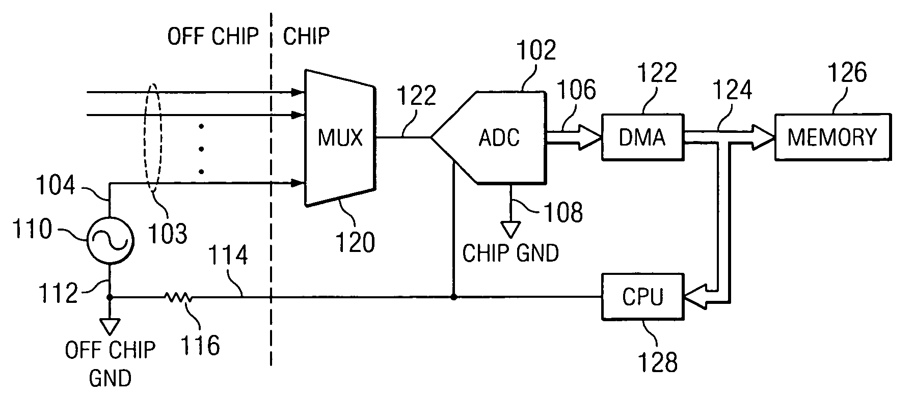
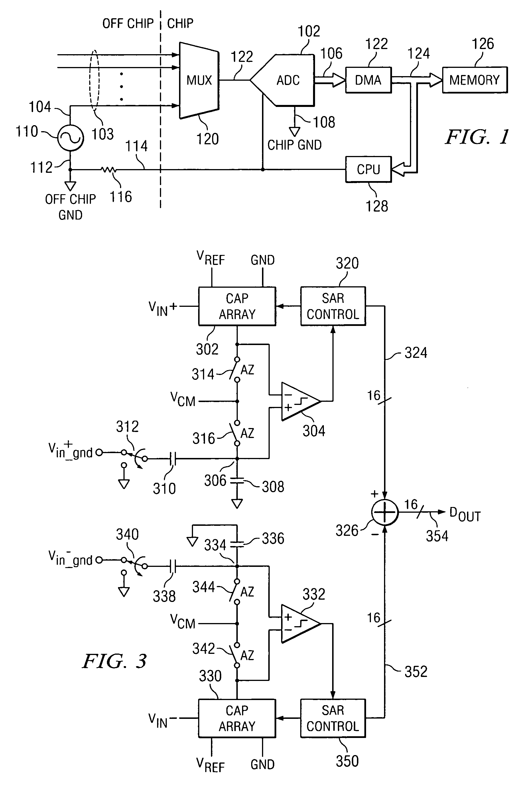
[0038]Referring now to FIG. 1, there is illustrated a diagrammatic view of a mixed signal integrated circuit that provides both processing functionality and the ability to sample external analog signals and convert them to digital information for storage on the integrated circuit. The analog signals are represented by a plurality of analog input data lines 103, of which one is illustrated as being connected to an external signal source 110. Signal source 110 is referenced to an off chip ground node 112. This is connected through a resistor 116 to an input ground 114 connection to the integrated circuit, which will be described hereinbelow. The input analog lines are input to a multiplexer 120, which is operable to provide a single analog output 122 that is input to an analog-to-digital convertor (ADC) 102. The ADC 102 is operable to sample the analog signal at predetermined intervals at a predetermined sampling rate and convert the analog value at each sample to a digital value and ...


PUM


Abstract

DMA controller for mixed signal device. A mixed signal integrated circuit with memory control is disclosed. A data conversion circuit is provided that is operable to receive an analog input signal and convert discrete samples thereof at a predetermined sampling rate to a digital representations thereof as a plurality of digital words. A memory stores the digital words generated by the data conversion circuit. A processor is included on the integrated circuit and operable to access the memory to output select ones of the digital words for processing thereof in accordance with a predetermined processing algorithm. A memory access controller controls access to the memory by the data conversion circuit and the processor. The memory access controller is operable to restrict access to the memory by the data conversion circuit without interrupting the generation of digital words therefrom when the processor is accessing the memory, and allowing access to the memory by the data conversion circuitry when the processor is not accessing the memory, such that the data conversion circuit can transfer currently generated digital words and previously generated and non stored digital words for storage in said memory upon gaining access thereto.

Description

CROSS REFERENCE TO RELATED APPLICATIONS[0001]This application is Continuation-in-Part of U.S. patent application Ser. No. 10 / 453,369, filed Jun. 3, 2003 now U.S. Pat. No. 6,882,298, and entitled “SAR ANALOG-TO-DIGITAL CONVERTER WITH TWO SINGLE ENDED INPUTS,” and is related to co-pending application entitled “NOISE CANCELLATION IN A SINGLE ENDED SAR CONVERTER,” Ser. No. 10 / 753,163; and co-pending application entitled “SAR DATA CONVERTER WITH UNEQUAL CLOCK PULSES FOR MSBS TO ALLOW FOR SETTLING,” Ser. No. 10 / 734,890; and co-pending application entitled “HIGH SPEED COMPARATOR WITH BLOCKING SWITCHES FOR SAR CONVERTER,” Ser. No. 10 / 735,164; and co-pending application entitled “COMMON CENTROID LAYOUT FOR PARALLEL RESISTORS IN AN AMPLIFIER WITH MATCHED AC PERFORMANCE,” Ser. No. 10 / 735,387, all co-pending applications being Continuation-in-Part applications of U.S. patent application Ser. No. 10 / 453,369, filed Jun. 3, 2003, entitled “SAR ANALOG-TO-DIGITAL CONVERTER WITH TWO SINGLE ENDED INPU...

Claims


Application Information

Patent Timeline
Patent Type & Authority Patents(United States)
IPC IPC(8): G06F3/00H03M1/12G06F13/28H01C10/16H03M1/06H03M1/10H03M1/34H03M1/38H03M1/46H03M1/66H03M1/78
CPCH03M1/1057H03M1/468G06F13/28
Inventor LEUNG, KAFAILEUNG, KA Y.
Owner SILICON LAB INC
Why Eureka
Try Eureka