
Laser annealing mask and method for smoothing an annealed surface

Active Publication Date: 2007-03-20
SHARP KK
View PDF8 Cites 62 Cited by
  • Summary
  • Abstract
  • Description
  • Claims
  • Application Information

AI Technical Summary

Benefits of technology

[0015]The present invention method is used for smoothing the surface roughness of a silicon substrate during the crystallization process, using a surface “smoothing” mask feature. Making the substrate surface smooth enables improved TFT performance, with a simultaneous improvement in TFT reliability. The present invention process doesn't add time-consuming additional steps to the LILaC process.

Problems solved by technology

When forming thin film transistors (TFTs) for use in LCD or other microelectronic circuits, the location of transistors channel regions, the orientation of regular structured polycrystalline silicon (poly-Si) or single-grain-crystalline silicon, and the surface roughness are important issues.
The most important reason for this end result is the inability of conventional methods to achieve such quality differentiation.
In the case of conventional laser annealing, some differentiation is possible, but the price, in terms of loss of throughput, is very high for the modest performance gains realized.
Further, not all these processes can be location controlled.
This kind of non-uniformity is highly detrimental for critical-application TFTs where uniformity of characteristics is more essential than absolute performance.

Method used


Image

  • Laser annealing mask and method for smoothing an annealed surface
  • Laser annealing mask and method for smoothing an annealed surface
  • Laser annealing mask and method for smoothing an annealed surface

Examples


Embodiment Construction

[0027]FIG. 4 is a plan view of the present invention laser annealing mask with sub-resolution aperture patterns. The mask 400 comprises at least one section 402 with aperture patterns for transmitting approximately 100% of incident light, and at least one section 404 with aperture patterns for diffracting incident light.

[0028]FIG. 5 depicts a variation of the sub-resolution mask of FIG. 4. As shown, mask 500 comprises a plurality of adjacent 100% transmission sections 502a, 502b, and 502c with aperture patterns for transmitting approximately 100% of incident light. Also shown, the mask 500 includes a plurality of adjacent sections 504a through 504f with aperture patterns for diffracting incident light. The number of adjacent 100% transmission sections typically varies between 2 and 5 (three are shown), although the present invention is not limited to any particular number. Likewise, the number of adjacent diffracting sections typically varies between 2 and 5. Such a mask would be us...


PUM

PropertyMeasurementUnit
Fractionaaaaaaaaaa
Fractionaaaaaaaaaa
Fractionaaaaaaaaaa

Abstract

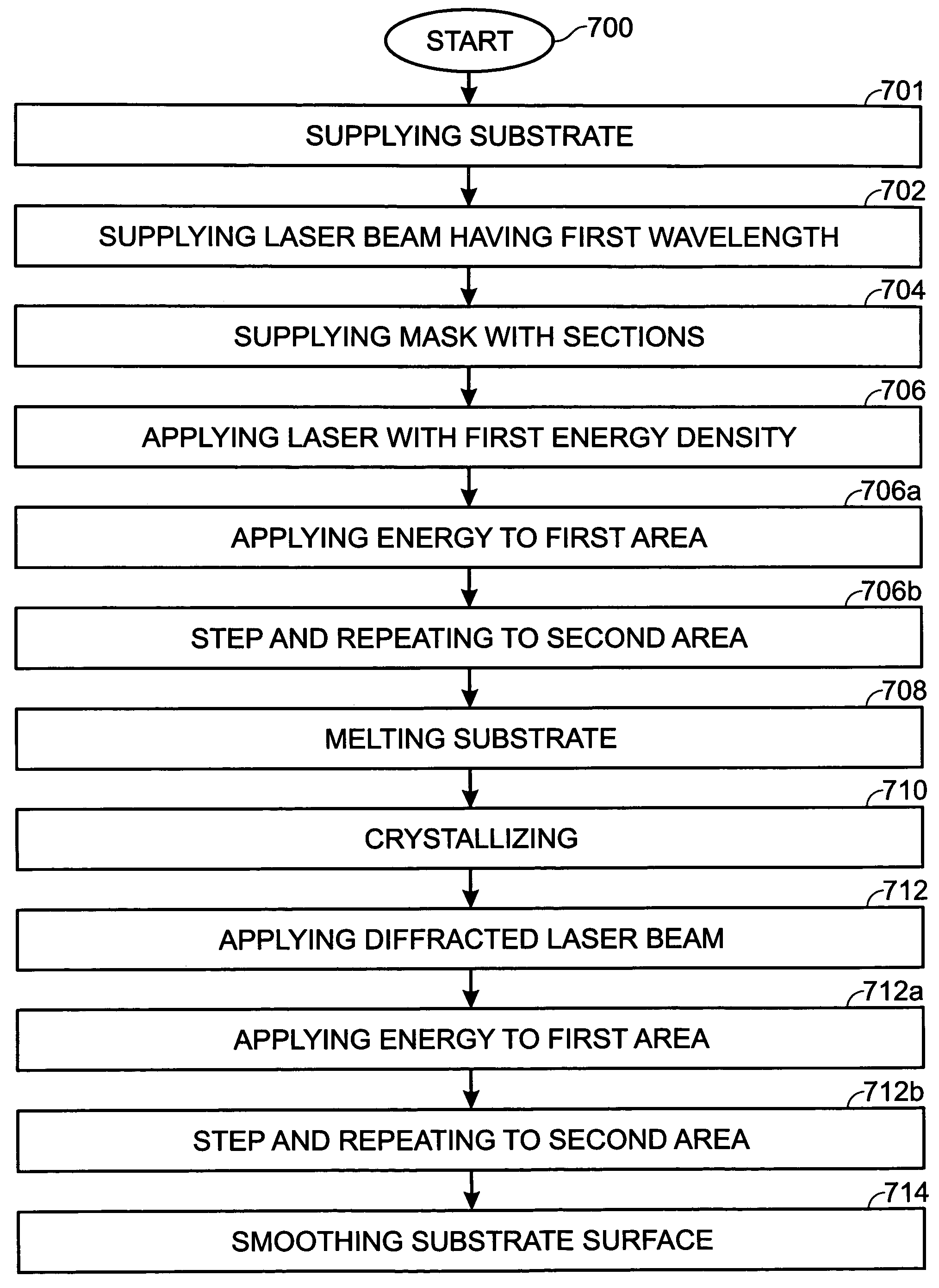
A mask with sub-resolution aperture features and a method for smoothing an annealed surface using a sub-resolution mask pattern are provided. The method comprises: supplying a laser beam having a first wavelength; supplying a mask with a first mask section having apertures with a first dimension and a second mask section with apertures having a second dimension, less than the first dimension; applying a laser beam having a first energy density to a substrate region; melting a substrate region in response to the first energy density; crystallizing the substrate region; applying a diffracted laser beam to the substrate region; and, in response to the diffracted laser beam, smoothing the substrate region surface. In some aspects of the method, applying a diffracted laser beam to the substrate area includes applying a diffracted laser beam having a second energy density, less than the first energy density, to the substrate region. The second energy density is in the range of 40% to 70% of the first energy density, and preferably in the range of 50% to 60% of the first energy density.

Description

BACKGROUND OF THE INVENTION[0001]1. Field of the Invention[0002]This invention generally relates to integrated circuit (IC) and liquid crystal display (LCD) fabrication and, more particularly, to a system and method for smoothing the surface of a crystallized substrate during a laser annealing process.[0003]2. Description of the Related Art[0004]When forming thin film transistors (TFTs) for use in LCD or other microelectronic circuits, the location of transistors channel regions, the orientation of regular structured polycrystalline silicon (poly-Si) or single-grain-crystalline silicon, and the surface roughness are important issues. This poly-Si material can be used as the active layer of poly-Si TFTs in the fabrication of active-matrix (AM) backplanes. Such backplanes can be used in the fabrication of AM LCDs and can be also combined with other display technologies, such as organic light-emitting diodes (OLEDs).[0005]Poly-Si material is typically formed by the crystallization of i...

Claims


Application Information

Patent Timeline
IPC IPC(8): H01L21/322B23K26/00B23K101/36C30B13/00H01L21/20H01L21/268
CPCC30B29/06C30B13/00
Inventor MITANI, YASUHIROVOUTSAS, APOSTOLOS T.CROWDER, MARK A.
Owner SHARP KK
Learn More