Method of forming MIM capacitor electrodes

a technology of metal insulation metal and capacitors, which is applied in the direction of capacitors, semiconductor devices, and semiconductor/solid-state device details, etc., can solve the problems of affecting the electrical performance of mim capacitors, unable or very difficult to construct ics with more than one or two layers of interconnects, and unable to achieve further layers. , to achieve the effect of preventing plasma-induced damage, improving the performance of mim capacitors, and improving the electrical performance of mim capacitor

Active Publication Date: 2007-04-03
TAIWAN SEMICON MFG CO LTD
View PDF5 Cites 7 Cited by
  • Summary
  • Abstract
  • Description
  • Claims
  • Application Information

AI Technical Summary

Benefits of technology

[0017]In accordance with these and other objects and advantages, the present invention is generally directed to a novel method for forming electrodes in the fabrication of an MIM (metal-insulator-metal) capacitor. The method improves MIM capacitor performance by preventing plasma-induced damage to a dielectric layer during deposition of a top electrode on the dielectric layer, as well as by reducing or preventing the formation of an interfacial layer between the dielectric layer and the electrode or electrodes, in fabrication of the MIM capacitor. The method typically includes the patterning of crown-type capacitor openings in a substrate; depositing a bottom electrode in each of the crown openings; subjecting the bottom electrode to a rapid thermal processing (RTP) or furnace anneal step; depositing a dielectric layer on the annealed bottom electrode; depositing a top electrode on the dielectric layer using a plasma-free CVD (chemical vapor deposition) or ALD (atomic layer deposition) process; and patterning the top electrode of each MIM capacitor.

Problems solved by technology

Only a relatively short time ago, it was impossible or very difficult to construct an IC with more than one or two layers of interconnects.
The topology variations created by forming multiple layers on top of one another resulted in such significant depth of focus problems with lithographic processes that any further additions of layers were nearly impossible to achieve.
Top electrode interaction with thin, high-k dielectric materials has been found to adversely impact the electrical performance of MIM capacitors, including excessive junction leakage and lower breakdown voltage.
Recent research indicates that the electrical performance of MIM capacitors is strongly correlated with plasma damage induced in the dielectric layer during deposition of the top electrode on the dielectric layer.
This is particularly problematic with regard to dielectric layers which are fabricated using high-k dielectric materials.

Method used


Image

  • Method of forming MIM capacitor electrodes
  • Method of forming MIM capacitor electrodes
  • Method of forming MIM capacitor electrodes

Examples


Embodiment Construction

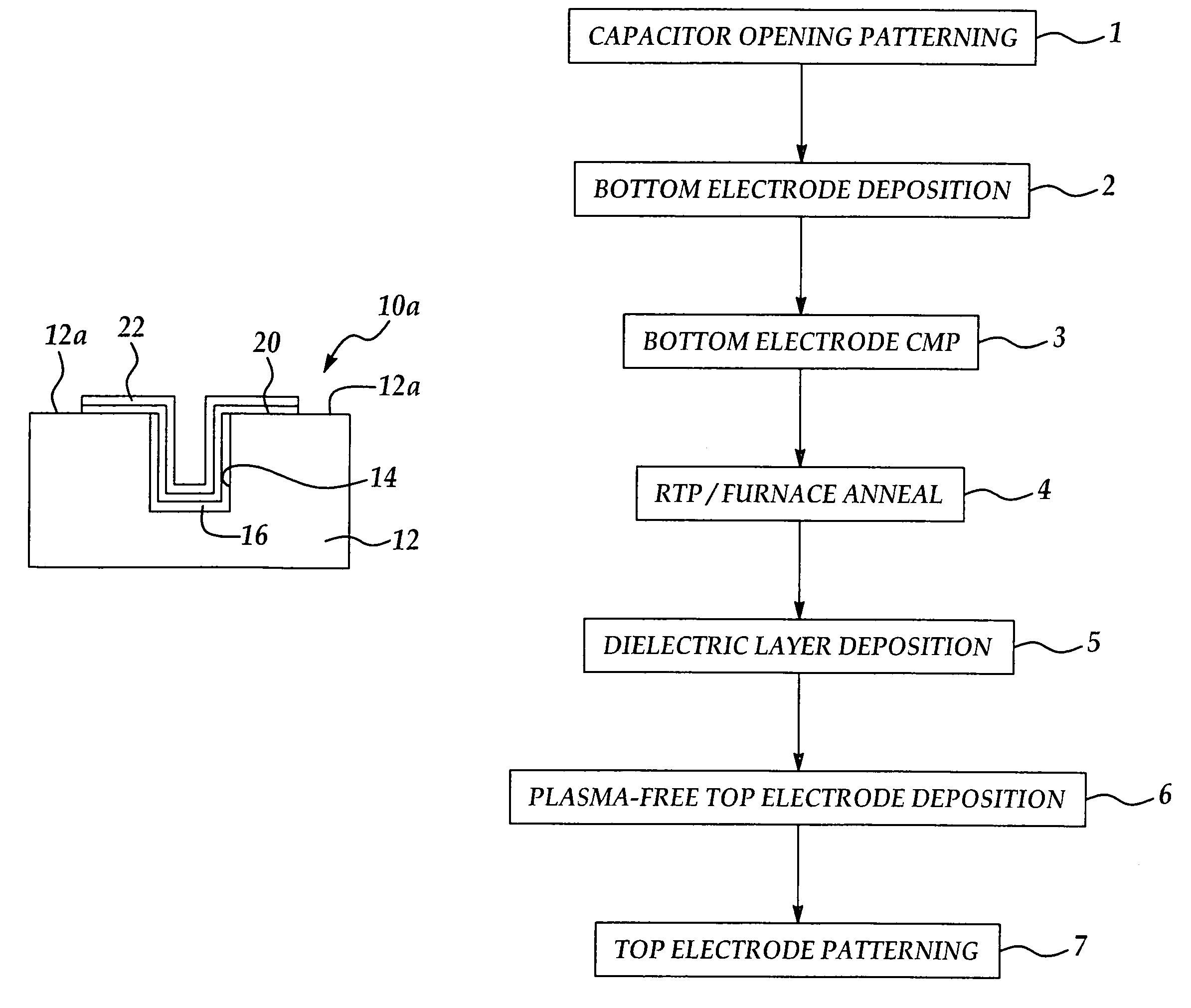
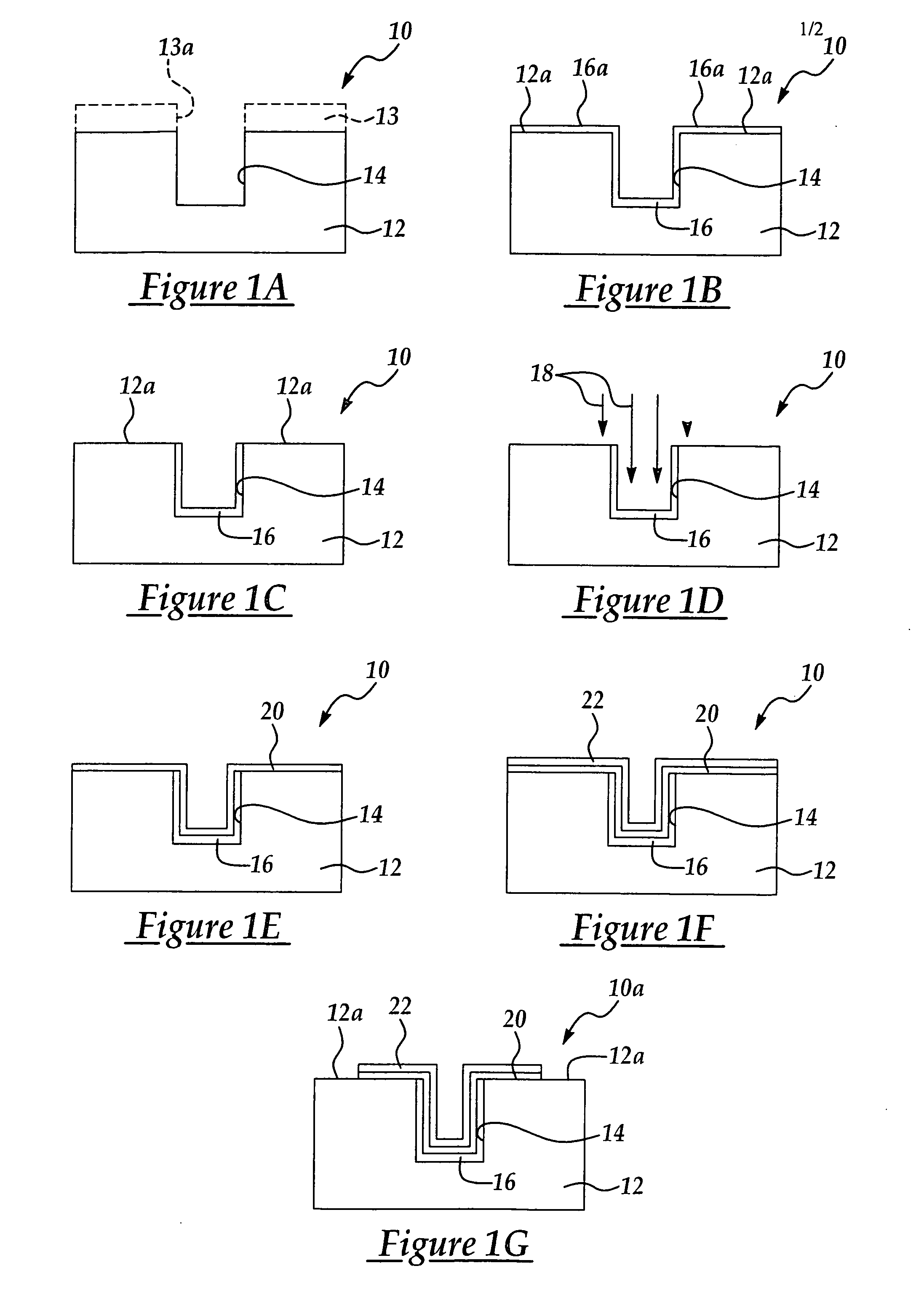
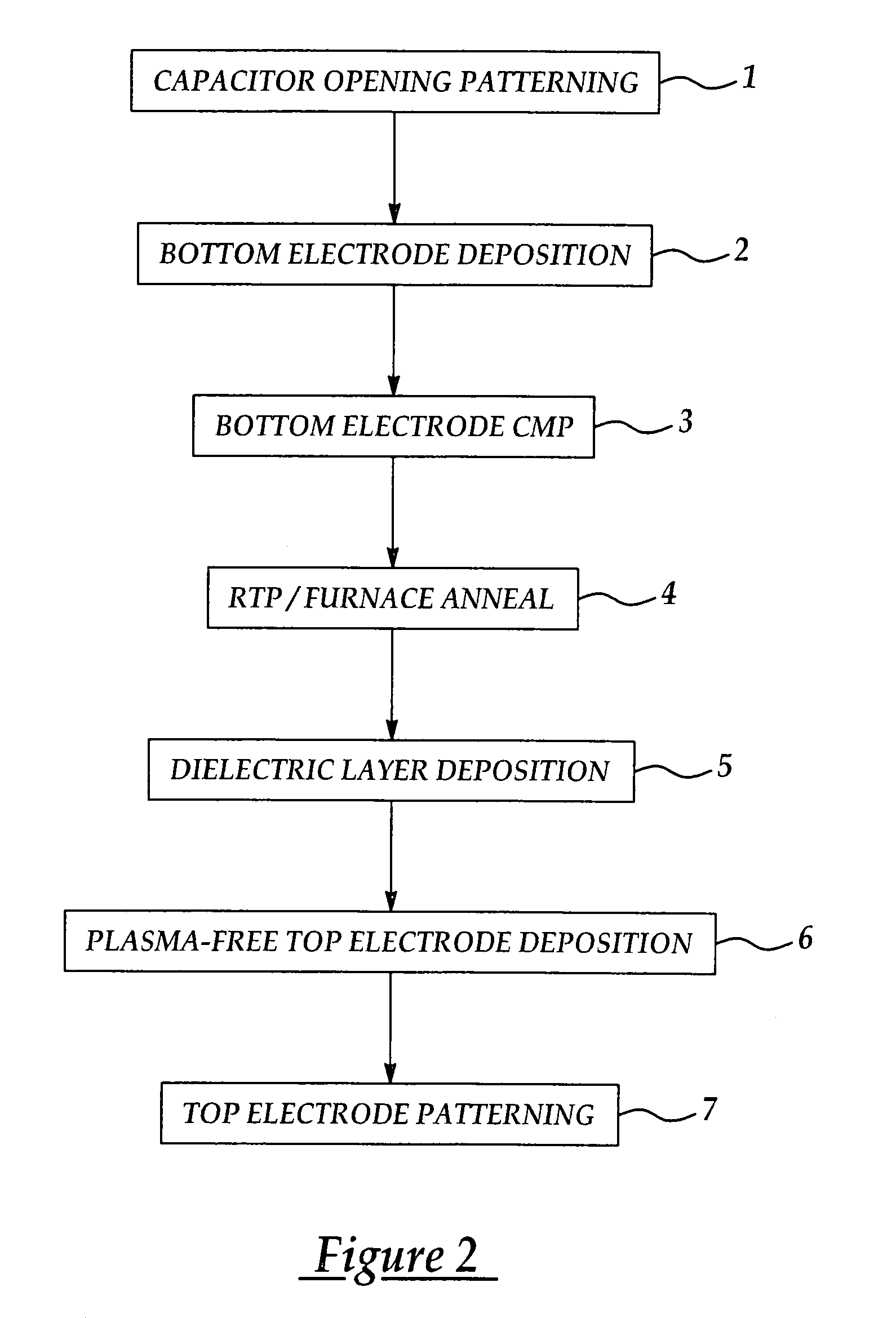
[0021]The present invention generally contemplates a novel method for forming electrodes in the fabrication of an MIM (metal-insulator-metal) capacitor. The method improves the electrical performance of an MIM capacitor by preventing plasma-induced damage to a high-k dielectric layer as a top electrode is deposited on the dielectric layer during fabrication of the capacitor. The method of the invention further improves capacitor performance by reducing or preventing the formation of an interfacial layer between the dielectric layer and a top electrode and a bottom electrode during fabrication of the capacitor.

[0022]In a typical process flow according to the method of the present invention, crown-type capacitor openings are initially patterned in a substrate. A bottom electrode, typically TiN, is then deposited in each of the capacitor openings. The bottom electrode is subjected to a rapid thermal processing (RTP) or furnace anneal step, after which a dielectric layer is deposited on...


PUM


Abstract

A novel method for forming electrodes in the fabrication of an MIM (metal-insulator-metal) capacitor, is disclosed. The method improves MIM capacitor performance by preventing plasma-induced damage to a dielectric layer during deposition of a top electrode on the dielectric layer, as well as by reducing or preventing the formation of an interfacial layer between the dielectric layer and the electrode or electrodes, in fabrication of the MIM capacitor. The method typically includes the patterning of crown-type capacitor openings in a substrate; depositing a bottom electrode in each of the crown openings; subjecting the bottom electrode to a rapid thermal processing (RTP) or furnace anneal step; depositing a dielectric layer on the annealed bottom electrode; depositing a top electrode on the dielectric layer using a plasma-free CVD (chemical vapor deposition) or ALD (atomic layer deposition) process; and patterning the top electrode of each MIM capacitor.

Description

FIELD OF THE INVENTION[0001]The present invention relates to methods for fabricating MIM (metal-insulator-metal) capacitors on a semiconductor wafer substrate. More particularly, the present invention relates to an MIM capacitor electrode fabrication method in which a top electrode is formed using a plasma-free deposition process at relatively low temperature to reduce or prevent electrical performance degradation of the capacitor.BACKGROUND OF THE INVENTION[0002]In the fabrication of semiconductor integrated circuits, metal conductor lines are used to interconnect the multiple components in device circuits on a semiconductor wafer. A general process used in the deposition of metal conductor line patterns on semiconductor wafers includes deposition of a conducting layer on the silicon wafer substrate; formation of a photoresist or other mask such as titanium oxide or silicon oxide, in the form of the desired metal conductor line pattern, using standard lithographic techniques; subje...

Claims


Application Information

Patent Timeline
Patent Type & Authority Patents(United States)
IPC IPC(8): H01L21/8242H01G4/005H01L21/02H01L21/28H01L21/3205H01L21/44H01L23/522H01L29/06
CPCH01L23/5223H01L28/60H01L2924/0002H01L2924/00
Inventor WU, CHIH-TALIN, KUO-YINHUANG, TSUNG-HSUNYU, CHUNG-YICHAO, LAN-LINTU, YEUR-LUENLIN, HSING-LIENTSAI, CHIA-SHIUNG
Owner TAIWAN SEMICON MFG CO LTD
Why Eureka
Try Eureka