Window interface layer of a light-emitting diode

a technology of light-emitting diodes and window layers, which is applied in the direction of laser details, active medium materials, semiconductor devices, etc., can solve the problems of affecting the operational life of components, affecting the efficiency of light emitted from the side of the die, and affecting the lattice mismatch of gaas of 3.6%, so as to improve the film quality of the window layer, reduce dislocation defects, and enhance luminous intensity

Inactive Publication Date: 2007-04-03
ARIMA OPTOELECTRONICS
View PDF2 Cites 5 Cited by
  • Summary
  • Abstract
  • Description
  • Claims
  • Application Information

AI Technical Summary

Benefits of technology

[0011]A primary object of the invention is to provide a window interface layer of a light-emitting diode that employs a p-GaInP interface layer interposed between a p-GaP window layer and a p-AlGaInP cladding layer to reduce the dislocation defects, thereby improving the film quality of the window layer and enhancing the luminous intensity as well as having an excellent forward voltage Vf.
[0012]Another object of the invention is to provide a window interface layer of a light-emitting diode in which the p-GaInP interface layer can be continuously formed by using the MOCVD process after the AlGaInP layers are deposited one after another. Meanwhile, a p-GaP window layer can also be continuously deposited by use of the MOCVD process after the interface layer is grown. In this way, the interface layer and the window layer are formed in the same state except the growth temperature, thereby simplifying the manufacturing process.

Problems solved by technology

However, GaP and GaAs have a lattice mismatch of 3.6%.
However, the use of the material of GaAsP or GaP in the window layer results in lattice mismatch with the substrate, thereby affecting the operational life time of the components.
However, the light emitted from the side of the die can't be effectively utilized in the case of an optimal thickness ranging from 0.1 to 5 μm, thereby limiting the luminous efficiency of the light-emitting diodes.

Method used


Image

  • Window interface layer of a light-emitting diode
  • Window interface layer of a light-emitting diode
  • Window interface layer of a light-emitting diode

Examples


Embodiment Construction

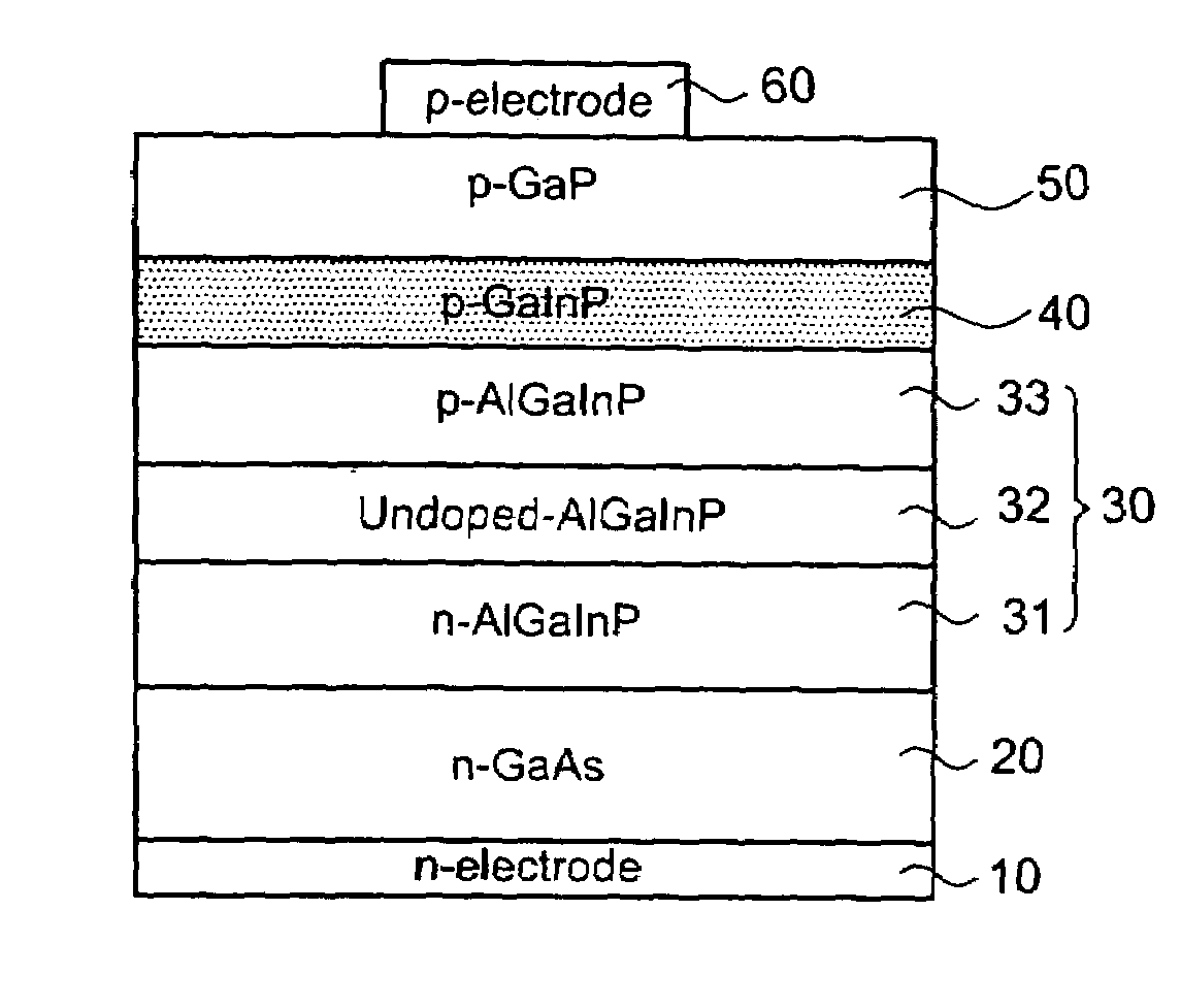
[0028]First of all, referring to FIG. 5, a substrate 20 in accordance with the invention is made of n-type GaAs or the like. An AlGaInP double hetero structure 30 lies on the topside of the n-type GaAs substrate 20. The AlGaInP double hetero structure 30 consists of an n-type AlGaInP cladding layer 31 formed atop the n-type GaAs substrate 20, an undoped AlGaInP active layer 32 atop the cladding layer 31, and a p-AlGaInP cladding layer 33 atop the active layer 32. The aforementioned three layers are deposited one after another by use of the Metal-Organic Chemical Vapor Deposition (MOCVD) process. In accordance with the invention, the undoped AlGaInP active layer 32 constitutes an AlGaInP multi-quantum well (MQW).

[0029]A highly doped p-type interface layer 40 is made of GaxIn1-xP (0.6≦x≦0.9) and formed atop the p-AlGaInP cladding layer 33. Thereafter, a p-type window layer 50 made of p-GaP is formed atop the interface layer 40. The deposition of the interface layer 40 is adapted to re...


PUM


Abstract

This invention is about a window interface layer in a light-emitting diode which comprises an n-type GaAs substrate with an n-type ohmic electrode at the bottom side thereof; an n-type AlGaInP cladding layer formed atop the substrate; an undoped AlGaInP active layer formed atop the n-type cladding layer; a p-AlGaInP cladding layer formed atop the active layer; a p-type window layer made of GaP; a p-type ohmic electrode formed atop the p-type window layer; and a highly doped p-type interface layer made of GaxIn1-xP (0.6≦x≦0.9) and interposed between the p-type cladding layer and p-type window layer wherein the highly doped p-GaInP interface layer possesses a band gap which is higher than that of the active layer and, however, smaller than that of the p-type cladding layer, and wherein the lattice constant lies between GaAs and GaP. In this way, the p-GaInP interface layer is interposed between a p-GaP window layer and a p-AlGaInP cladding layer for enhancing the film quality and the luminous efficiency as well as improving the electric property.

Description

BACKGROUND OF THE INVENTION[0001]1. Field of the Invention[0002]The invention relates to a window interface layer of a light-emitting diode, and more particularly to a p-GaInP interface layer interposed between a p-GaP window layer and a p-AlGaInP layer for enhancing the film quality and the luminous efficiency as well as improving the electric property.[0003]2. Description of the Related Art[0004]With the rapid development of the Metal-Organic Chemical Vapor Deposition (MOCVD), the MOCVD process has been widely applied to the production of AlGaInP material with excellent crystallization. Accordingly, it is suitable for the mass production of light-emitting diodes with high luminance.[0005]The conventional AlGaInP light-emitting diode is formed on an n-type GaAs substrate with a double heterostructure (DH). The double heterostructure includes a p-AlGaInP and an n-type AlGaInP cladding layer at a top and a bottom side while a luminous active layer is interposed between the cladding l...

Claims


Application Information

Patent Timeline
Patent Type & Authority Patents(United States)
IPC IPC(8): H01L29/06H01L31/0328H01L31/0336H01L31/072H01L31/109H01L33/02H01L33/14
CPCH01L33/02H01L33/14
Inventor WANG, PEI-JIHWU, RUPERT
Owner ARIMA OPTOELECTRONICS
Why Eureka
Try Eureka