

Method for manufacturing high-transmittance optical filter for image display devices
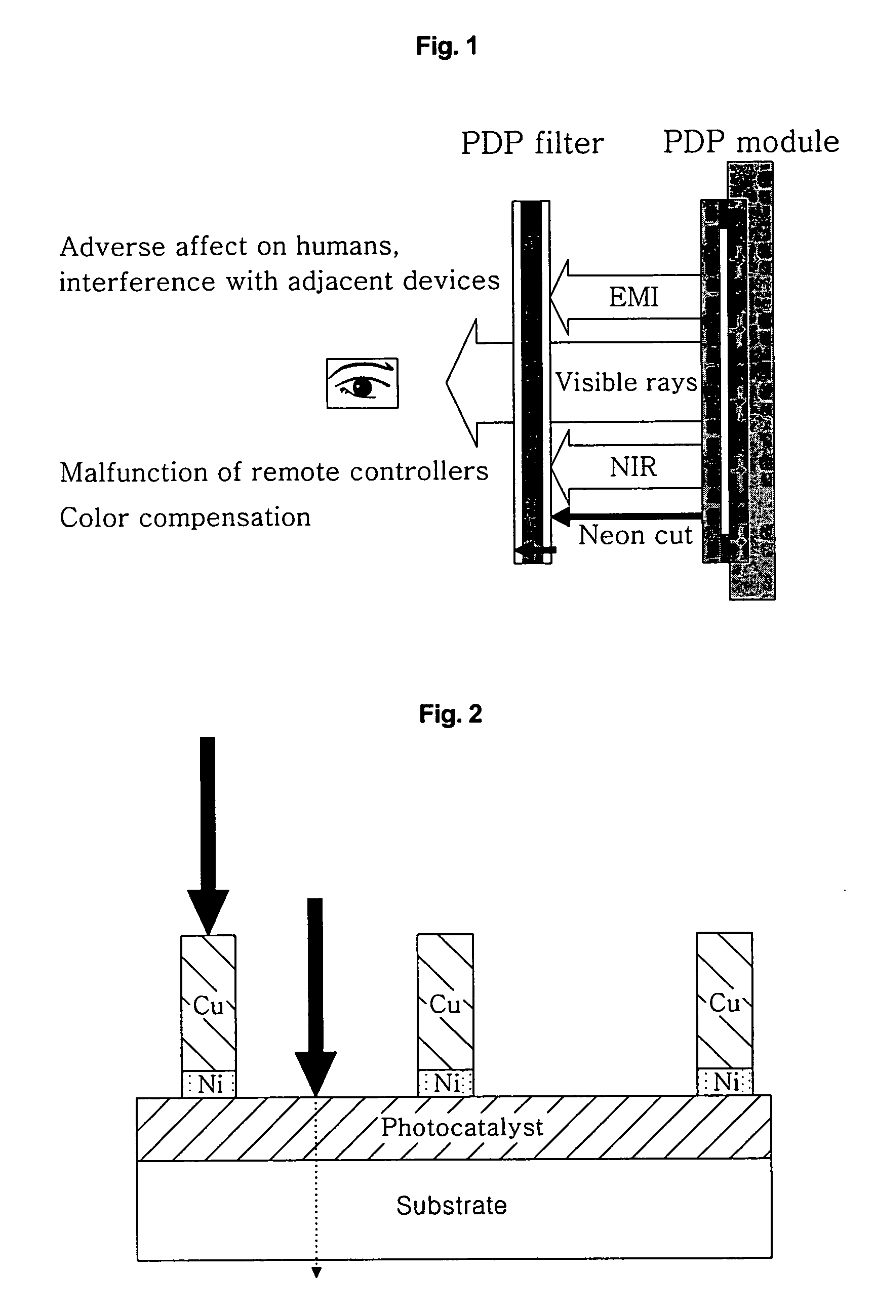
a technology of image display device and high-transmittance optical filter, which is applied in the direction of photosensitive material processing, photomechanical equipment, instruments, etc., can solve the problems of insufficient electromagnetic wave shielding effect without a reduction in transparency, inability to achieve high transparency without a deterioration in electromagnetic wave shielding performance, and inability to achieve sufficient electromagnetic wave shielding effect. , to achieve the effect of increasing the transmittance of the metal pattern
- Summary
- Abstract
- Description
- Claims
- Application Information
AI Technical Summary
Benefits of technology
Problems solved by technology
Method used
Image

Examples
examples
[0054]Embodiments of the present invention will now be described in more detail with reference to the following examples. However, these examples are given for the illustration of the preferred embodiments of the present invention only, and are not to be construed as limiting the scope of the invention.
examples 1 and 2
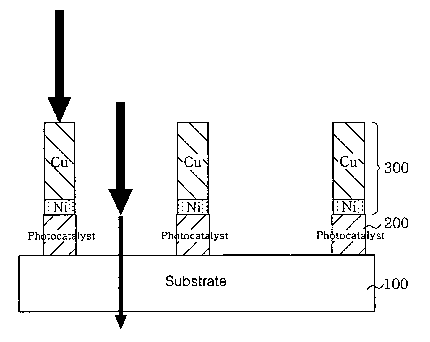
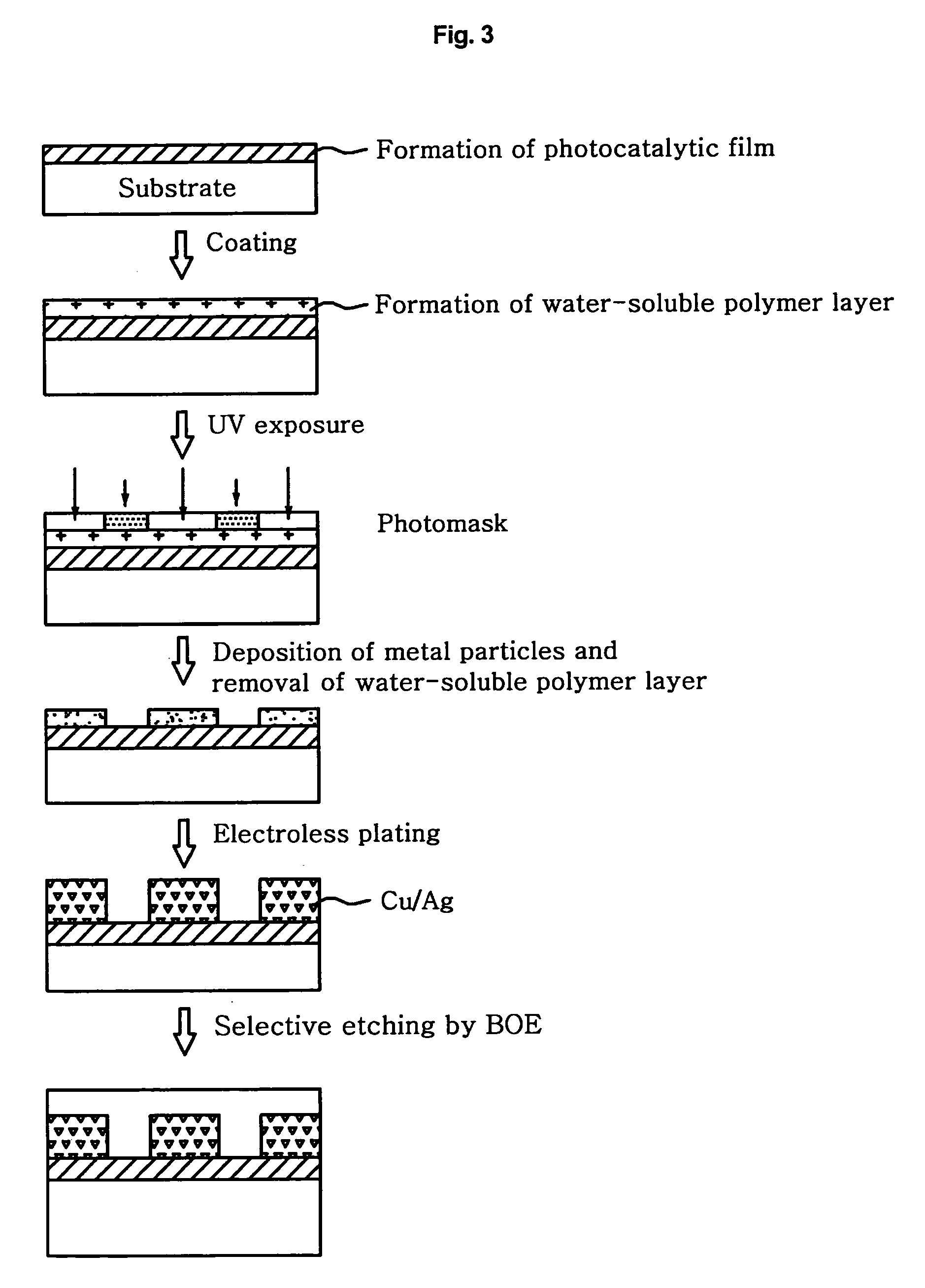
[0055]A solution of polybutyl titanate (2.5 wt %) in isopropanol was applied to a transparent glass substrate by spin coating, and was then dried at 150° C. for 5 minutes to form an amorphous TiO2 film. At this time, the TiO2 film was controlled to have a thickness of 30 mm to 100 nm. Thereafter, triethanol amine as a photosensitizer was added to an aqueous solution of 5 wt % of polyvinylalcohol (Mw: 25,000). At this time, the photosensitizer was used in an amount of 1% by weight, based on the weight of the polymer. The resulting mixture was stirred, coated on the TiO2 film, and dried at 60° C. for 2 minutes. Next, UV light having a broad wavelength range was irradiated to the coated substrate through a photomask on which a fine mesh pattern was formed using a UV exposure system (Oriel, U.S.A). After the exposure, the substrate was dipped in a solution of PdCl2 (0.6 g) and HCl (1 ml) in water (1 liter) to deposit Pd particles on the surface of the exposed portion. As a result, a neg...
PUM
| Property | Measurement | Unit |
|---|---|---|
| temperature | aaaaa | aaaaa |
| thickness | aaaaa | aaaaa |
| temperature | aaaaa | aaaaa |
Abstract
Description
Claims
Application Information