Method of forming a surface acoustic wave (SAW) filter device

a surface acoustic wave and filter device technology, applied in the direction of conductive pattern formation, generator/motor, waveguide, etc., can solve the problems of poor electromechanical coupling, high temperature drift, and prevent the use of saw devices, and achieve the effect of facilitating thermal diffusion

Inactive Publication Date: 2007-05-08
TRIQUINT
View PDF9 Cites 128 Cited by
  • Summary
  • Abstract
  • Description
  • Claims
  • Application Information

AI Technical Summary

Benefits of technology

[0005]The present invention may be described by way of example with an embodiment including a SAW filter which includes an electrode pattern deposited on a piezoelectric substrate having a strong electromechanical coupling characteristic, which substrate is bonded at near room temperature to a surrogate substrate through an intermediate catalytic layer to provide desirable temperature compensation for the SAW filter. A very low built in stress level is exhibited at the bonding area, thereby reducing wafer breakage during the fabrication process and improving reliability of the SAW device. The piezoelectric substrate may be Lithium Tantalate or alternatively Lithium Niobate, used with a surrogate substrate of an inorganic Silicon (Si) material. The intermediate layer is comprised of a silicon oxide material. The pre-selected thickness of the silicon oxide material layer provides isolation to a capacitance coupling between the electrode pattern and the Silicon substrate, which in use may be attached to a base. Since Si has a very good thermal conductivity, it improves thermal diffusion through the substrate thereby increasing the power handling capability and reducing the pyro-sensitivity of the SAW device. Yet another embodiment of the invention provides a SAW filter comprising an electrode pattern on a piezoelectric substrate that is bonded to a surrogate substrate through an intermediate bonding layer wherein the thickness of the piezoelectric substrate, the thickness of the bonding layer, the bulk resistivity of the surrogate substrate, and the stress level of the bond area may be changed to adjust the temperature coefficient and passband characteristics of the SAW filter.
[0006]One embodiment of the present invention may be described for a surface acoustic wave (SAW) device comprising a piezoelectric substrate having a thickness at least twice an acoustic wavelength of a SAW, a surrogate substrate characterized by an expansion coefficient less than that of the piezoelectric substrate, and a thermal conductivity for facilitating thermal diffusion, and a catalytic bonding film securing the piezoelectric substrate to the surrogate substrate. The catalytic bonding film having a thickness of at least one micron provides isolation between the two substrates to effectively reduce the electrode pattern capacitance coupling. The device will have an expansion coefficient less than that of the piezoelectric substrate.
[0008]A method aspect of the invention may include forming a surface acoustic wave (SAW) filter device. One method comprises providing a piezoelectric substrate having a thickness at least twice an acoustic wavelength of a SAW, polishing a surface of the piezoelectric substrate, depositing a silicon oxide film onto the surface of the piezoelectric substrate, and polishing an exposed film surface of the silicon oxide film deposited on the piezoelectric substrate. A surrogate substrate is provided that is characterized by an expansion coefficient less than that of the piezoelectric substrate and a thermal conductivity for facilitating thermal diffusion. The method includes polishing one surface of the surrogate substrate, depositing a silicon oxide film onto the one surface of the surrogate substrate, and polishing an exposed surface of the silicon oxide film deposited on the surrogate substrate. While at a normal temperature, the exposed film surfaces of the silicon oxide films are compressed against each other with a force sufficient for bonding the piezoelectric substrate to the surrogate substrate. As desired, transducers are formed on an exposed surface of the piezoelectric substrate.

Problems solved by technology

Lithium Niobate and Lithium Tantalate have strong electromechanical coupling but generally suffer from high temperature drift, whereas Quartz has stable temperature characteristics but poor electromechanical coupling.
However, the relatively high temperature drift associated with these substrates typically precludes their use in SAW devices for certain applications that require a very high close-in rejection.
While SAW filters are significantly smaller than comparable ceramic filters, the temperature drift of SAW devices on high coupling substrates such as Lithium Tantalate and Lithium Niobate make them undesirable for PCS duplexer application.
If not properly controlled, the pyroelectric effect may cause damage to the SAW device during the manufacturing process, thus reducing yield and reliability of the device.
However, these methods suffer from a major drawback in which the SAW properties depend upon the thickness of the SiO2 film.
So while it is possible to demonstrate extremely good temperature performance, the SAW device is highly dispersive and thus prohibits the use of these techniques in production.
This structure as disclosed by Taguchi has a major drawback in the performance of the filter passband characteristics.
Thus, while the structure may provide better temperature characteristics, it suffers with a significant degradation in filter passband performance.
This would result in higher insertion loss and a narrowing of the passband that renders them unsuitable for mobile applications.

Method used


Image

  • Method of forming a surface acoustic wave (SAW) filter device
  • Method of forming a surface acoustic wave (SAW) filter device
  • Method of forming a surface acoustic wave (SAW) filter device

Examples


Embodiment Construction

[0019]The present invention will now be described more fully with reference to the accompanying drawings in which various embodiments of the invention are shown and described. It is to be understood that the invention may be embodied in many different forms and should not be construed as limited to the illustrated embodiments set forth herein. Rather, these embodiments are provided so that this disclosure will be thorough and complete, and will convey the scope of the invention to those skilled in the art. Like numbers refer to like elements.

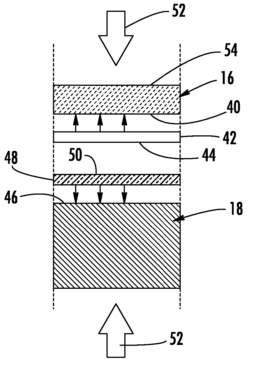
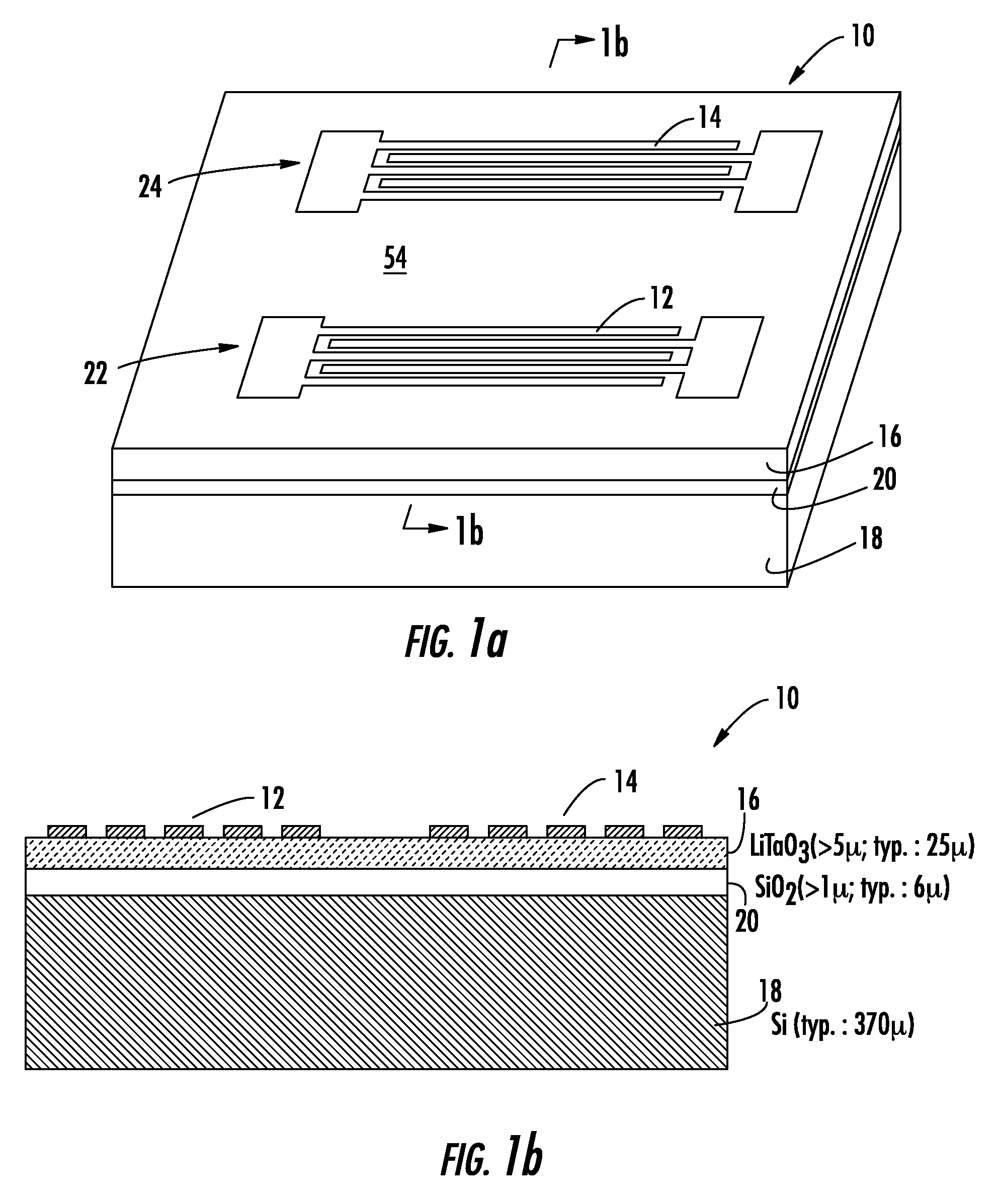
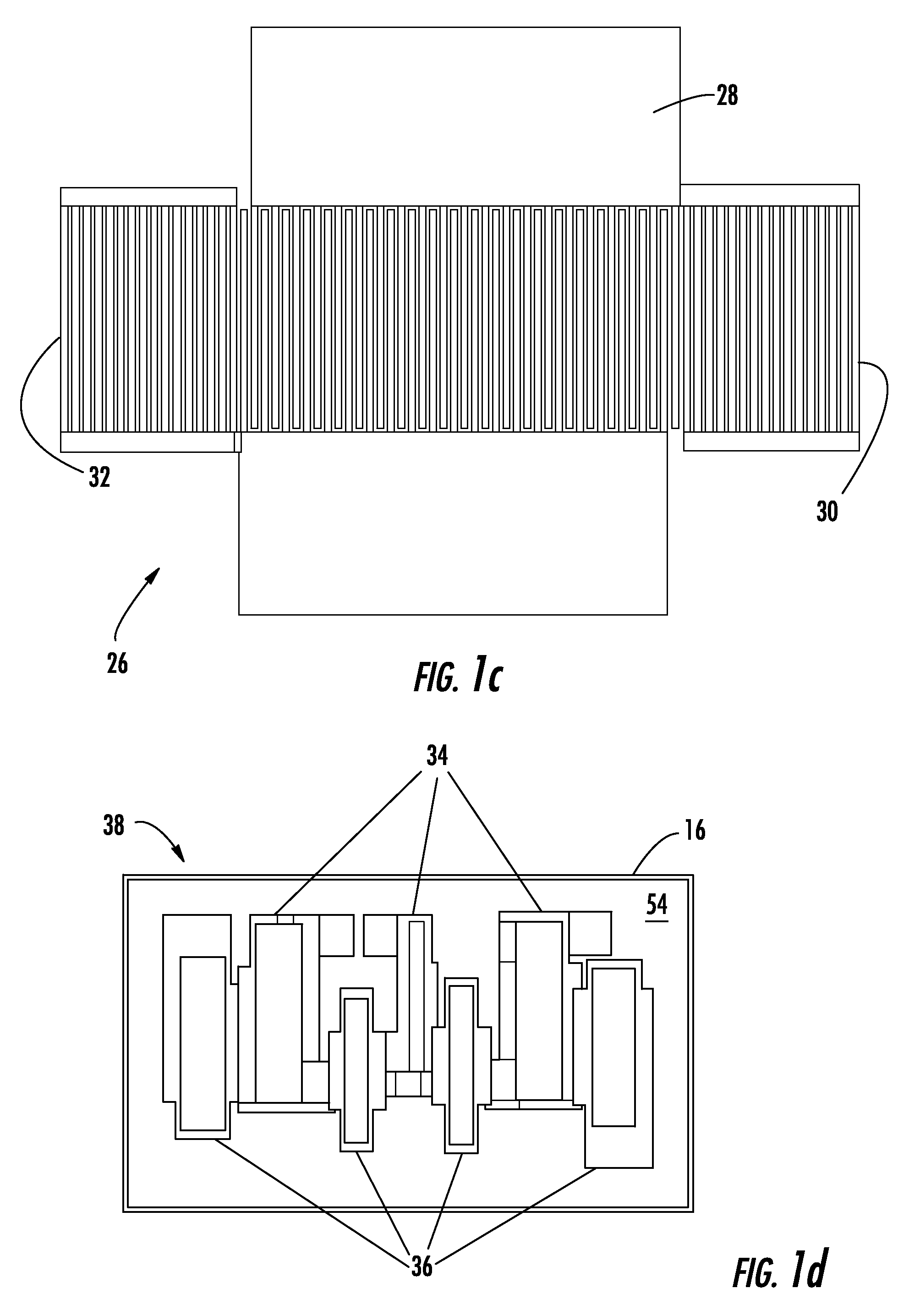
[0020]One embodiment of the present invention, a SAW filter 10 illustrated with reference to FIG. 1 includes electrode patterns 12, 14 deposited on a piezoelectric substrate 16, which substrate is bonded to a surrogate substrate 18 through a bonding layer 20 of a Silicon oxide material (SiOx). FIG. 1b illustrates a cross section of the composite device of FIG. 1. The electrode patterns 12, 14 form transducers 22, 24 that may be composed of inter...


PUM


Abstract

A SAW filter includes a piezoelectric substrate of Lithium Niobate or optionally Lithium Tantalate having a thickness of at least twice an acoustic wavelength. The piezoelectric substrate is bonded to a surrogate substrate of a silicon material. The surrogate substrate is characterized by a resisitivity of at least 100 ohm-cm and an expansion coefficient compatible with the piezoelectric substrate. A catalytic bonding film between the piezoelectric substrate and the surrogate substrate is formed from a first catalytic bonding film deposited onto a surface of the piezoelectric substrate and a second catalytic bonding film deposited onto a surface of the surrogate substrate. The piezoelectric substrate is bonded to the surrogate substrate through a compression force sufficient for providing a bonding at a normal temperature.

Description

CROSS-REFERENCE TO RELATED APPLICATIONS[0001]This application is a Divisional application of U.S. application Ser. No. 10 / 454,797, filed Jun. 4, 2003 now U.S. Pat. No. 7,105,980 which claims the benefit of U.S. Provisional Application No. 60 / 393,527, filed Jul. 3, 2002, the disclosures of which are herein incorporated by reference in their entirety.FIELD OF THE INVENTION [0002]The present invention relates to surface acoustic wave devices useful for applications in wireless communications.BACKGROUND OF THE INVENTION [0003]Surface acoustic wave devices are commonly used in wireless communications for meeting system-filtering requirements. Generally, surface acoustic wave (SAW) filters are manufactured by forming interdigital transducers on piezoelectric substrates such as Lithium Niobate, Lithium Tantalate, Quartz, or the like. Lithium Niobate and Lithium Tantalate have strong electromechanical coupling but generally suffer from high temperature drift, whereas Quartz has stable tempe...

Claims


Application Information

Patent Timeline
Patent Type & Authority Patents(United States)
IPC IPC(8): H04R17/00H01L41/00H03H9/00H02N2/00H03H3/08H03H3/10H03H9/02H03H9/64
CPCH03H3/08H03H9/02094H03H9/02559H03H9/02566H03H9/02574H03H9/02834H03H9/02897H03H9/02952H03H9/02984H03H9/6489H03H3/10Y10T29/42Y10T29/49005Y10T29/49155Y10T29/49002Y10T29/49156
Inventor ABBOTT, BENJAMIN P.MALOCHA, SVETLANACHOCOLA, JACKMONETTI, GARYZEPESS, JOSHUA M.
Owner TRIQUINT
Why Eureka
Try Eureka