Semiconductor device

a technology of semiconductors and devices, applied in the field of semiconductor devices, can solve the problems of reducing the current output to the drain electrode, not being suitable for use as a switch for the power source system, and not being suitable for the use of the third electrode as a switch, etc., and achieve the effect of reducing the leakage current to the third electrod

Active Publication Date: 2007-05-15
PANASONIC CORP
View PDF5 Cites 36 Cited by
  • Summary
  • Abstract
  • Description
  • Claims
  • Application Information

AI Technical Summary

Benefits of technology

[0016]According to the aforementioned configuration, by taking the configuration where the barrier layer is made to be thin only directly under the third electrode, VP can have a positive value, a short-circuit does not occur between the first and second electrodes in the state where the voltage is not applied to the third electrode with respect to the first electrode. At the same time, since there exists the barrier layer having the same thickness as that of the conventional HFET at the location other than directly under the third electrode, the maximum current value Imax has never been changed from that conventionally achieved, while the higher transconductance gm compared with that of the conventional general HFET can be achieved and a leakage current to the third electrode can be reduced. In other words, a channel is completely depleted without the voltage being applied to the third electrode (gate electrode) with respect to the first electrode (source electrode), while a gate-source channel and a gate-drain channel are not depleted and the insulating film layer can be formed under the gate electrode. Hence, as compared with the HFET using the conventional group III nitride semiconductor, VP can have a positive value, high Imax and gm can be achieved, and a gate leakage current can be reduced.
[0033]According to the aforementioned configuration, when a metal such as nickel (Ni), palladium (Pd), palladium silicon (PdSi), platinum (Pt), or gold (Au) is used as a material of the third electrode, a Schottky barrier of the third electrode can be set higher than the conventional are, thereby the leakage current to the third electrode can be reduced.

Problems solved by technology

In the normally-on mode, even when the voltage applied to the gate electrode is 0 V, a current flows through the source and drain electrodes, so that the source and drain electrodes are short-circuited even during a power failure, and as a result, it is not suitable for use as a switch for the power source system.
The reason that it is preferable to have a leakage current in the HFET be as small as possible is because, when the leakage current flows through the gate electrode, a current output to the drain electrode is reduced and the current flows through a region where the current inherently should not flow, resulting in a problem with the operation of a circuit or the like.
It is, however, impossible to satisfy the four performance indexes of the HFET described above at once in the HFET that uses the conventional group III nitride semiconductor.

Method used


Image

  • Semiconductor device
  • Semiconductor device
  • Semiconductor device

Examples


first embodiment

[0047](First Embodiment)

[0048]Referring to FIG. 1A through FIG. 1F, a semiconductor device according to a first embodiment of the present invention will be described.

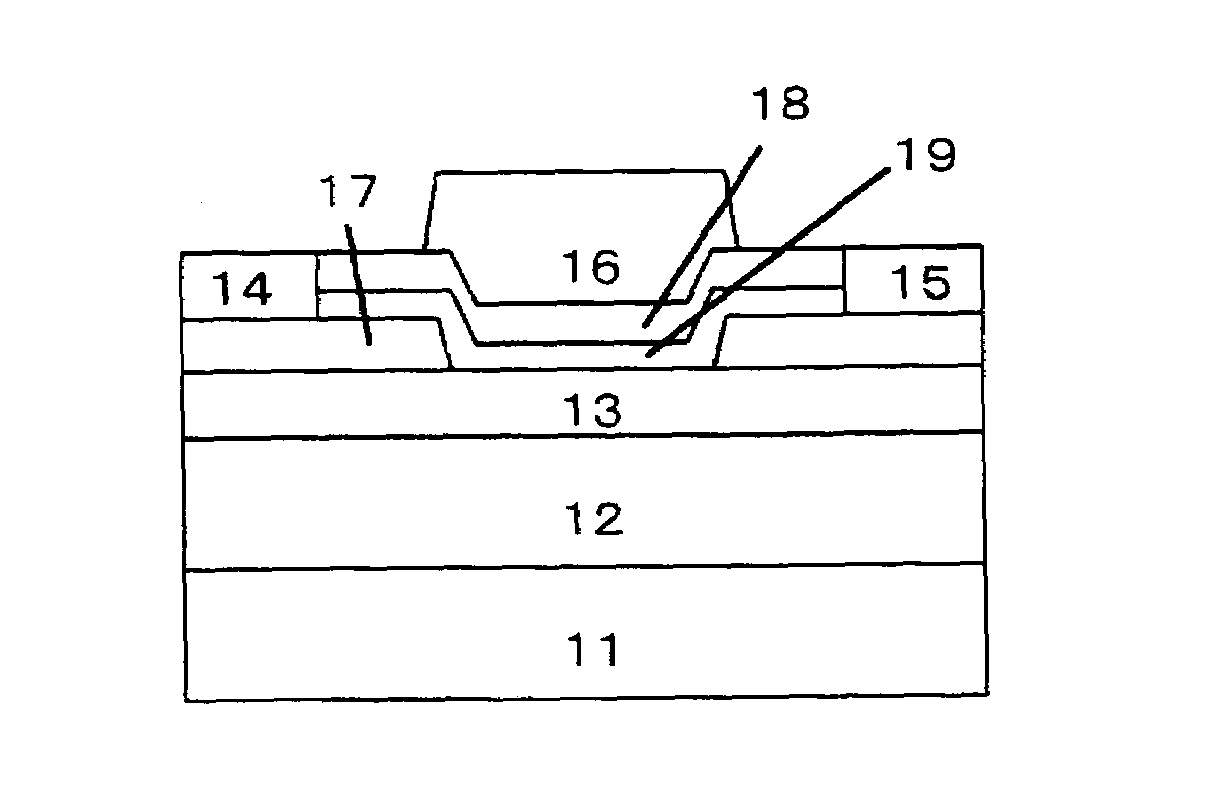
[0049]FIG. 1A schematically shows a cross section of the semiconductor device according to the present embodiment.

[0050]As shown in FIG. 1A, on an operation layer 12 composed of GaN formed on a substrate 11, a barrier layer 13 composed of AlxGa(1-x)N (012 directly under a gate electrode is higher than a Fermi energy in that location is stacked, and a heterojunction interface is formed of the operation layer 12 and the barrier layer 13. On the barrier layer 13, a semiconductor layer 17 composed of AlyGa(1-y)N(014 and a drain ohmic electrode 15 are formed thereon apart from each other, an insulating film 18 is formed between the source ohmic electrode 14 and the drain ohmic electrode 15, and a gate electrode 16 is formed thereon. It should be noted that, in the present embodiment, the semiconductor layer 17 is not stacked...

second embodiment

[0061](Second Embodiment)

[0062]Referring to FIG. 2A and FIG. 2B, a second embodiment according to the present invention will now be described. The second embodiment, which is obtained by further improving the first embodiment, makes it possible to achieve the normally-off mode and obtain a high breakdown voltage.

[0063]FIG. 2A schematically shows a cross section of a semiconductor device according to the second embodiment.

[0064]As shown in FIG. 2A, on the operation layer 12 composed of GaN formed on the substrate 11, a barrier layer 13 composed of AlxGa(1-x)N (012 directly under a gate electrode is higher than a Fermi energy in that location is stacked, and a heterojunction interface is formed of the operation layer 12 and the barrier layer 13. On the barrier layer 13, a semiconductor layer 17 composed of AlyGa(1-y)N (014 and a drain ohmic electrode 15 are formed thereon apart from each other, an insulating film 19 having a high dielectric breakdown voltage is formed between the sour...

third embodiment

[0067](Third Embodiment)

[0068]Referring to FIG. 3A through FIG. 3C, a semiconductor device according to a third embodiment of the present invention will be now described.

[0069]FIG. 3A schematically shows a cross section of the semiconductor device according to the present embodiment.

[0070]As shown in FIG. 3A, a barrier layer 13 composed of AlxGa(1-x)N (012 composed of GaN formed on a substrate 11, and a heterojunction interface is formed of the operation layer 12 and the barrier layer 13. On the barrier layer 13, a source ohmic electrode 14 and a drain ohmic electrode 15 are formed apart from each other, a semiconductor layer 20 (x>y) composed of AlyGa(1-y)N (014 and the drain ohmic electrode 15, where the AlyGa(1-y)N (012 directly under a gate electrode is higher than a Fermi energy in that location, and has an aluminum composition ratio smaller than that of the barrier layer 13, and a gate electrode 16 is formed thereon.

[0071]The configuration of the semiconductor device according...


PUM


Abstract

It is an object of the present invention to provide a semiconductor device, which can simultaneously achieve a normally-off mode of HFET and an improvement in Imax, and further achieve an improvement in gm and a reduction in gate leakage current. In order to keep a thin barrier layer 13 on an operation layer 12 of a substrate 11 directly under a gate electrode for mostly contributing to achieve the normally-off mode and also implement the high Imax, it is configured in such a way that a thickness of the barrier layer 13 can be increased by the semiconductor layer 17 between gate and source regions and between gate and drain regions. It is therefore possible to achieve the normally-off mode and an improvement in Imax as compared with an FET in which a thickness of the barrier layer is designed so as to be uniform. An insulating film 18 with a dielectric constant higher than that of the barrier layer is further inserted between a gate electrode 16 and the barrier layers 13, so that an improvement in gm and a reduction in gate leakage current can be achieved.

Description

BACKGROUND OF THE INVENTION[0001]1. Field of the Invention[0002]The present invention relates to a semiconductor device using a group III nitride semiconductor.[0003]2. Background Art[0004]A group III nitride semiconductor is a compound semiconductor composed of a compound of aluminum (Al), boron (B), gallium (Ga) or indium (In), and nitrogen (N), described by a general formula, BwAlxGayInzN (w+x+y+z=1; 0<=w, x, y, z<=1).[0005]Since the group III nitride semiconductor has advantages such as a large band gap and a high breakdown voltage accompanying therewith, a high electron saturated velocity and a high electron mobility, and a high concentration of electrons in a heterojunction, research and development thereof have been conducted to apply a group III nitride semiconductor to a short-wavelength light emitting device, a high-power high-frequency device, a high-frequency low-noise amplifying device, a power switch of a power source system, or the like. Especially, a heterojunc...

Claims


Application Information

Patent Timeline
Patent Type & Authority Patents(United States)
IPC IPC(8): H01L33/00
CPCH01L29/7786H01L29/2003
Inventor UENO, HIROAKIUEDA, TETSUZOUEMOTO, YASUHIROUEDA, DAISUKETANAKA, TSUYOSHIYANAGIHARA, MANABUHIROSE, YUTAKAHIKITA, MASAHIRO
Owner PANASONIC CORP
Why Eureka
Try Eureka