Superconducting filter

a superconducting filter and filter technology, applied in the direction of superconductors/hyperconductors, waveguides, resonators, etc., can solve the problems of large compatibility between both types, inability to easily make downsizing and good electric power characteristics, etc., and achieve the effect of reducing the reactive power of radio-frequency signals input and outputted to and from the superconducting filter, improving power characteristics, and easy circuit pattern impedance matching

Active Publication Date: 2007-05-15
FUJITSU LTD
View PDF15 Cites 21 Cited by
  • Summary
  • Abstract
  • Description
  • Claims
  • Application Information

AI Technical Summary

Benefits of technology

[0036]An object of the present invention is to provide a superconducting filter which can realize improved power characteristics with good repeatability and can be easily downsized.
[0038]According to the present invention, in the superconducting filter comprising: a dielectric substrate; a first input / output feeder formed on one surface of the dielectric substrate and formed of a superconductor film, for inputting a radio-frequency signal; a resonator pattern formed on said one surface of the dielectric substrate and formed of a superconductor film, for filtering the radio-frequency signal inputted from the first input / output feeder; a second input / output feeder formed on said one surface of the dielectric substrate and formed of a superconductor film, for outputting the radio-frequency signal filtered by the resonator pattern; and a dielectric body mounted on said one surface of the dielectric substrate with a plurality of spacers disposed therebetween, the dielectric body covers a region including the resonator pattern, the first input / output feeder over a length within ±20% of positive integer times a ¼ effective wavelength from a side nearer to the resonator pattern, and the second input / output feeder over a length within ±20% including ±20% of positive integer times the ¼ effective wavelength from a side nearer to the resonator pattern, whereby the superconducting filter can be small sized. The reflection of the radio-frequency signals can be depressed, and the impedance matching between the circuit patterns can be easily made. Thus, the reactive power of the radio-frequency signals inputted and outputted to and from the superconducting filter can be decreased, and the power characteristics can be improved.
[0039]Furthermore, according to the present invention, the dielectric body is mounted on one surface of the dielectric substrate by first spacers which are plastically deformable and secure the dielectric body mounted on one surface of the dielectric substrate and second spacers for defining the width of the gap between the dielectric substrate and the dielectric body, whereby the power characteristics can be improved with high repeatability.

Problems solved by technology

On the other hand, as for the transmission filter, which treats large electric power, the superconducting-type cannot easily make downsizing and good electric power characteristics, etc., such as power resistance, etc. compatible with each other.
The compatibility between both is a large problem.

Method used


Image

  • Superconducting filter
  • Superconducting filter
  • Superconducting filter

Examples


first embodiment

A First Embodiment

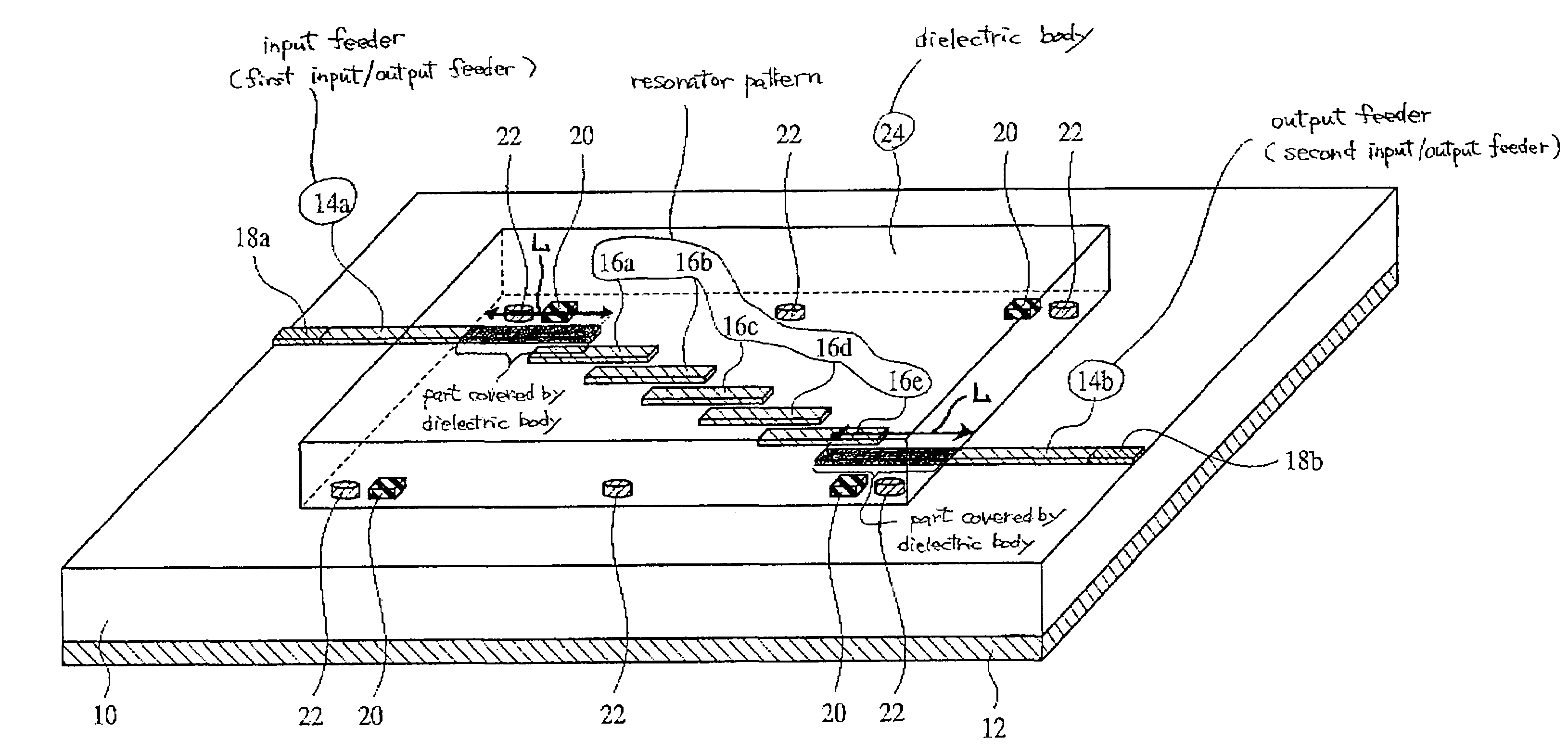
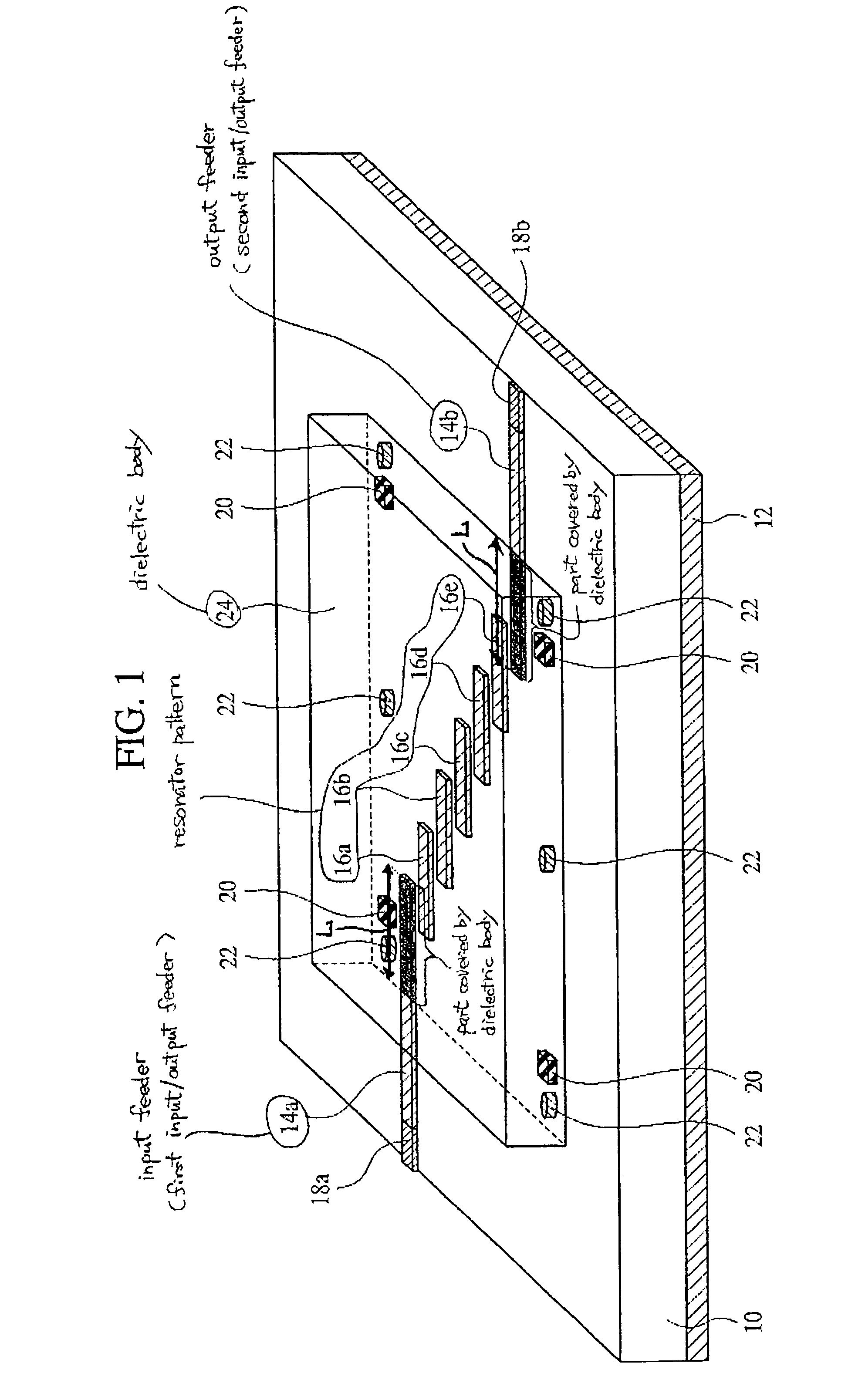
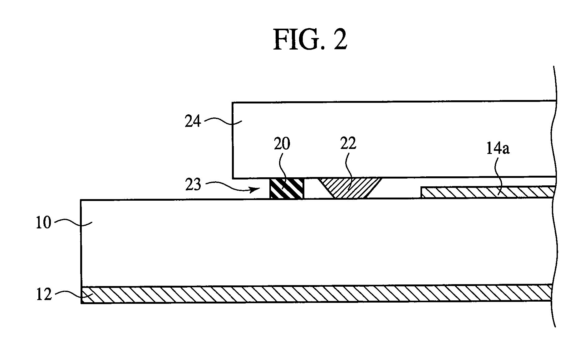
[0048]The superconducting filter according to a first embodiment of the present invention will be explained with reference to FIGS. 1 and 2. FIG. 1 is a perspective view of the superconducting filter according to the present embodiment, which illustrates a structure thereof. FIG. 2 is an enlarged sectional view of the structure of the superconducting filter according to the present embodiment, which illustrates the structure near the spacers.

[0049]The superconducting filter according to the present embodiment is a band-pass filter of the planar circuit type having the microstrip line transmission line structure and has an operational temperature of, e.g., below 100 K including 100 K.

[0050]As illustrated in FIG. 1, on the underside of a dielectric substrate 10 of magnesium oxide (110) single crystal, a ground plane 12 of a YBa2Cu3O7-δ (YBCO) superconductor film is deposited by, e.g., epitaxial growth.

[0051]On the upper surface of the dielectric substrate 10 there ar...

second embodiment

A Second Embodiment

[0077]The superconducting filter according to a second embodiment of the present invention will be explained with reference to FIG. 3. FIG. 3 is an enlarged sectional view of the superconducting filter according to the present embodiment, which illustrates the structure near spacers. The same members of the present embodiments as those of the superconducting filter according to the first embodiment are represented by the same reference numbers not to repeat or to simplify their explanation.

[0078]The basic structure of the superconducting filter according to the present embodiment is substantially the same as that of the superconducting filter according to the first embodiment. The superconducting filter according to the present embodiment is different from the superconducting filter according to the first embodiment in that in the former, the spacers 22 in the form of indium bumps are sandwiched by metal pads formed respectively on the upper surface of the dielect...

third embodiment

A Third Embodiment

[0084]The superconducting filter according to a third embodiment of the present invention will be explained with reference to FIGS. 4 and 5. FIG. 4 is a perspective view of the superconducting filter according to the present embodiment, which illustrates a structure thereof. FIG. 5 is an enlarged sectional view of the superconducting filter according to the present embodiment, which illustrates the structure near spacers.

[0085]The superconducting filter according to the present embodiment is a band-pass filter of the planar circuit type having the coplanar waveguide structure, and the operating temperature is, e.g., below 100 K including 100 K.

[0086]As illustrated in FIG. 4, a pair of ground planes 42a, 42b are formed on the upper surface of a dielectric substrate 40 of magnesium oxide, spaced from each other. The ground planes 42a, 42b are formed of DyBa2Cu3O7-δ (DyBCO) superconductor film deposited by, e.g., epitaxial growth.

[0087]In the region of the upper surfa...


PUM

PropertyMeasurementUnit
operational temperatureaaaaaaaaaa
temperaturesaaaaaaaaaa
dielectric constantaaaaaaaaaa

Abstract

A superconducting filter including input / output feeders formed on one surface of a dielectric substrate, resonator patterns formed on one surface of the dielectric substrate, and a dielectric plate mounted on the one surface of the dielectric substrate with a plurality of spacers formed on said one surface of the dielectric substrate disposed therebetween. The dielectric plate covers the region including the resonator patterns, and the input / output feeders length-wise over the length within ±20% of positive integer times a ¼ effective wavelength from the sides nearer to the resonator patterns.

Description

CROSS-REFERENCE TO RELATED APPLICATIONS[0001]This application is based upon and claims priority of Japanese Patent Application No. 2004-149271, filed on May 19, 2004, the contents being incorporated herein by reference.BACKGROUND OF THE INVENTION[0002]1. Field of the Invention[0003]The present invention relates to a superconducting filter for radio-frequency signals.[0004]2. Description of the Related Art[0005]Various radio-frequency filters are used at mobile communication stations, etc. which treat signals of a some GHz frequency region. As the reception filter of the radio-frequency filters used in the mobile communication stations, etc., coaxial resonator-type, dielectric resonator-type, superconducting resonator-type, etc. are known. The reception filters of these types are required to realize downsizing and higher frequency selectivity.[0006]The superconducting-type reception filter including as the circuit conductor a superconductor of an oxide high temperature superconductor...

Claims


Application Information

Patent Timeline
Patent Type & Authority Patents(United States)
IPC IPC(8): H01P1/203H01L39/00H01B12/02H01P1/205H01P1/208H01P7/08
CPCH01P1/20336H01P1/20363H01P1/20381Y10S505/70Y10S505/866
Inventor YAMANAKA, KAZUNORINAKANISHI, TERUKAI, MANABUAKASEGAWA, AKIHIKO
Owner FUJITSU LTD
Why Eureka
Try Eureka