Display device and electronic apparatus having a wiring connected to a counter electrode via an opening portion in an insulating layer that surrounds a pixel electrode

a technology of counter electrodes and electronic equipment, which is applied in the direction of discharge tubes, luminescent screens, identification means, etc., can solve the problems of low heat resistance of the electroluminescent layer, degrading image quality, and unable to withstand high heat processing, so as to prevent the degradation of the light emitting element with time, improve reliability, and suppress the effect of variations in luminance due to transistor characteristics

Inactive Publication Date: 2007-05-29
SEMICON ENERGY LAB CO LTD
View PDF45 Cites 47 Cited by
  • Summary
  • Abstract
  • Description
  • Claims
  • Application Information

AI Technical Summary

Benefits of technology

[0014]A display device according to the invention comprises a light emitting element which includes a light emitting material sandwiched between a first electrode connected to an anode line and a second electrode connected to a cathode line. The display device also comprises a transistor whose channel portion is formed of an amorphous semiconductor. The display device further comprises a reverse bias voltage applying circuit which switches potentials of the anode line and the cathode line with each other to apply a reverse bias voltage to the light emitting element. According to such a structure, degradation of the light emitting element with time can be prevented, leading to the display device with an improved reliability.
[0015]A display device according to the invention comprises a light emitting element which includes a light emitting material sandwiched between a pair of electrodes, a first transistor whose gate electrode is connected to a first power supply with a constant potential, and a second transistor whose gate electrode is connected to a signal line. The light emitting element, the first transistor, and the second transistor are connected in series between a second power supply with the same potential as a low potential voltage and a third power supply with the same potential as a high potential voltage

Problems solved by technology

However, the electro luminescent layer has a low heat resistance and can not withstand a high heat processing.
Therefore, due to different resistance values, a vol

Method used


Image

  • Display device and electronic apparatus having a wiring connected to a counter electrode via an opening portion in an insulating layer that surrounds a pixel electrode
  • Display device and electronic apparatus having a wiring connected to a counter electrode via an opening portion in an insulating layer that surrounds a pixel electrode
  • Display device and electronic apparatus having a wiring connected to a counter electrode via an opening portion in an insulating layer that surrounds a pixel electrode

Examples


embodiment mode 1

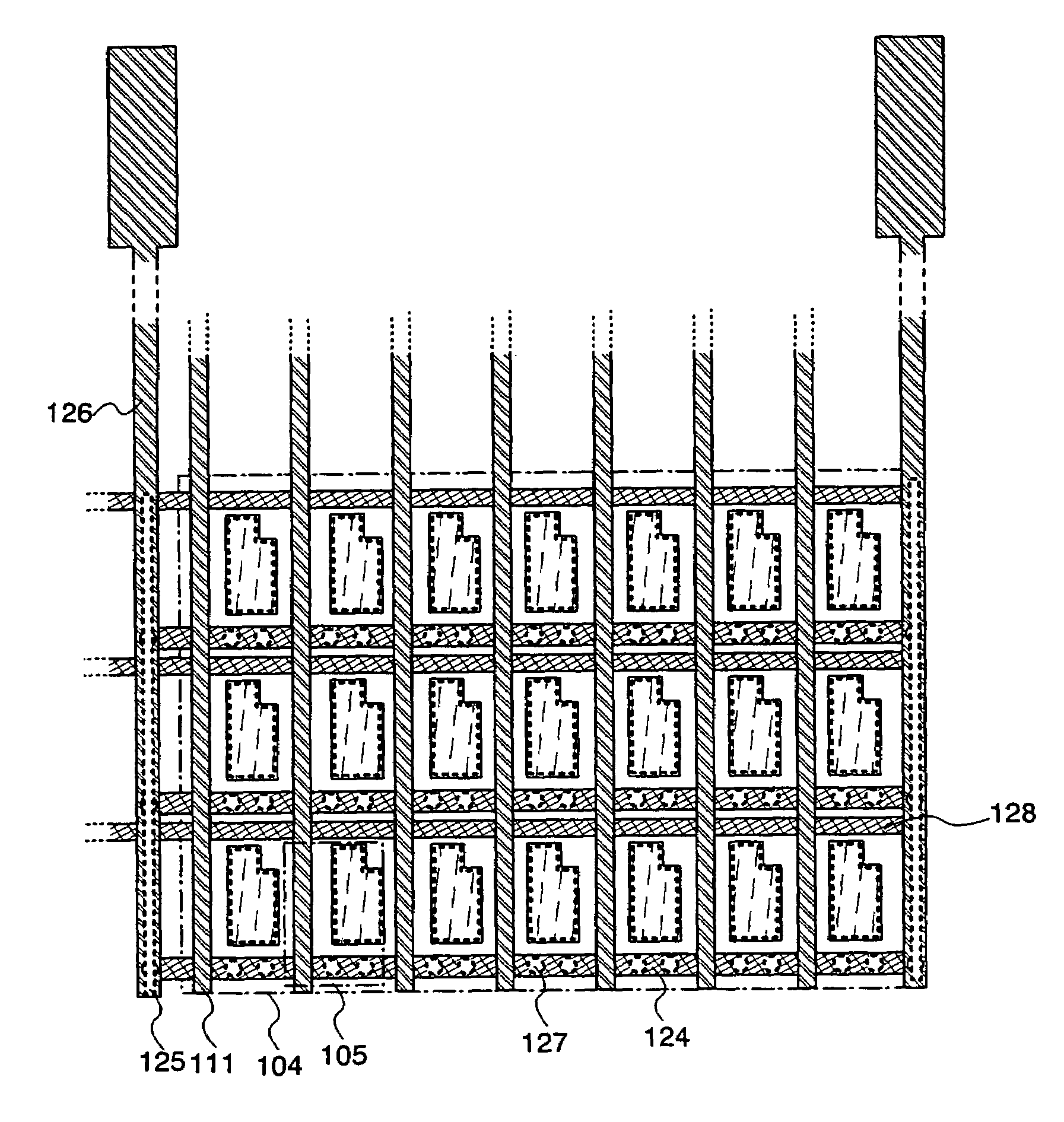
[0041]With reference to FIGS. 4A and 4B, explanation is made on an arrangement of wirings on a panel, especially an arrangement of a power supply line (hereinafter referred to as an anode line) with the same potential as a high potential voltage VDD, and a power supply line (hereinafter referred to as a cathode line) with the same potential as a low potential voltage VSS. It is to be noted that only wirings arranged in columns in a pixel portion 104 are shown in FIGS. 4A and 4B.

[0042]FIG. 4A is a top plan view of a panel comprising a substrate 100. On the substrate 100, the pixel portion 104 in which a plurality of pixels 105 arranged in matrix, a signal line driver circuit 101 arranged at the periphery of the pixel portion 104, and scan line driver circuits 102 and 103 are disposed. The number of driver circuits is not exclusively limited, and may be changed in accordance with a configuration of the pixel 105. Further, the driver circuits are not necessarily formed integrally on th...

embodiment mode 2

[0071]An embodiment mode of the invention is described with reference to drawings.

[0072]FIG. 8A is a top plan view of a panel which includes a substrate 200 having an insulating surface. On the substrate 200, a scan line driver circuit 203 and a pixel portion 202 including a plurality of pixels 201 arranged in matrix are formed. A plurality of driver ICs 205 are attached on the substrate 200, and the plurality of driver ICs 205 correspond to a signal line driver circuit 204. The scan line driver circuit 203 and the signal line driver circuit 204 are connected to a power supply circuit 206 and a controller 207.

[0073]The power supply circuit 206 supplies power to the panel, and is connected specifically to a power supply line disposed in the pixel portion 202. The power supply line is also referred to as an anode line or a cathode line. The anode line has the same potential as a high potential voltage VDD and the cathode line has the same potential as a low potential voltage VSS. The ...

embodiment mode 3

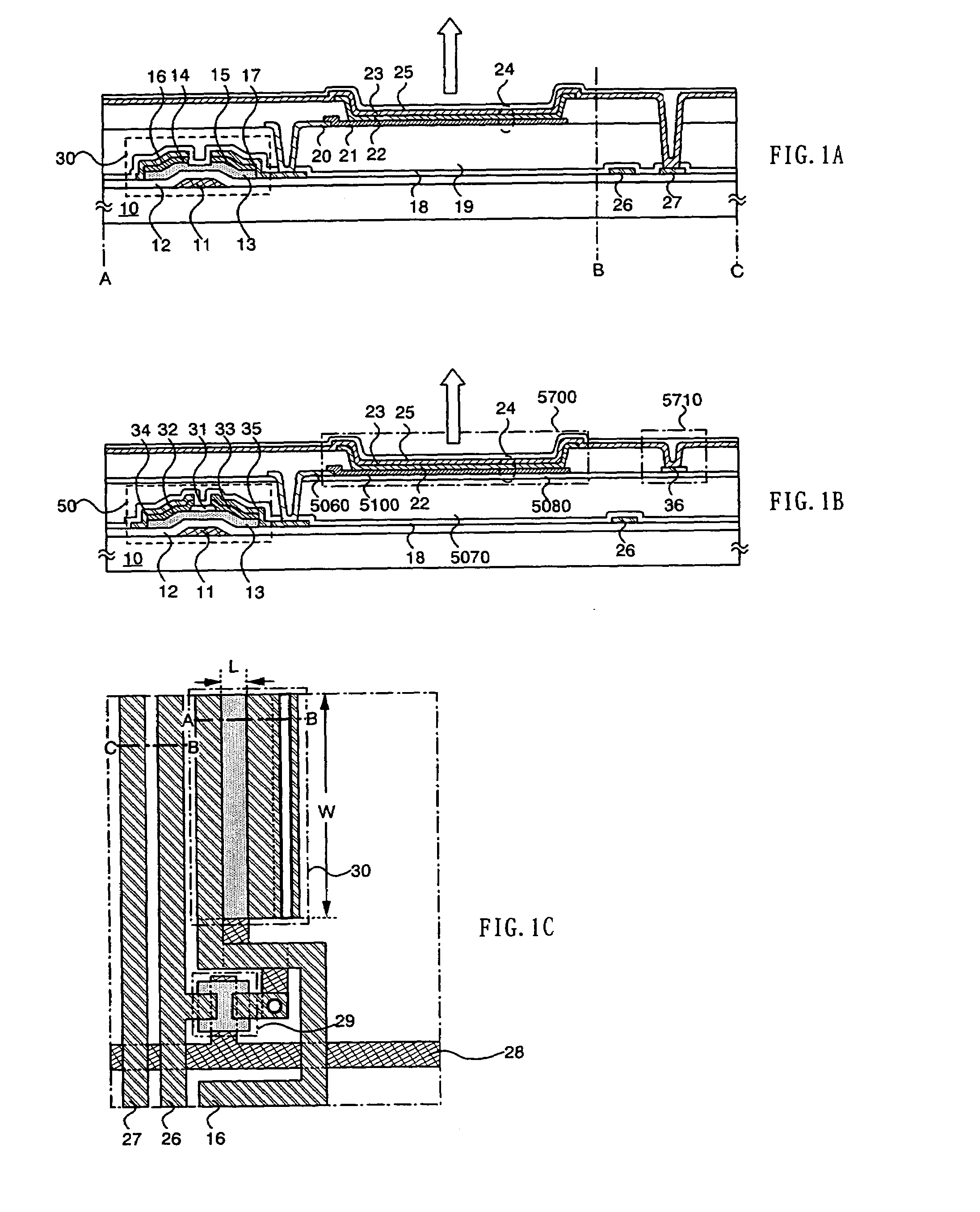
[0080]In this embodiment mode, a cross sectional structure of a CMOS circuit including an N-type transistor whose channel portion is formed of an amorphous semiconductor and a P-type transistor whose channel portion is formed of an organic semiconductor will be described with reference to FIGS. 10A and 10B.

[0081]FIG. 10A is an equivalent circuit diagram including a P-type transistor 221 and an N-type transistor 222 which are connected in series, and one terminal of which has the same potential as VDD and the other has the same potential as VSS. FIG. 10B is a cross sectional view of these transistors. In FIG. 10B, conductors 231 and 232 are formed on the substrate 200, and a silicon nitride 233 is formed thereon. Then, an amorphous semiconductor 234 is formed on the silicon nitride 233, and another silicon nitride 241 is formed thereon. On the silicon nitride 241, an N-type semiconductor and a conductor are laminated in this order, and then patterned simultaneously to form N-type sem...


PUM


Abstract

A display device in which variations in luminance due to variations in characteristics of transistors are reduced, and image quality degradation due to variations in resistance values is prevented. The invention comprises a transistor whose channel portion is formed of an amorphous semiconductor or an organic semiconductor, a connecting wiring connected to a source electrode or a drain electrode of the transistor, a light emitting element having a laminated structure which includes a pixel electrode, an electro luminescent layer, and a counter electrode, an insulating layer surrounding an end portion of the pixel electrode, and an auxiliary wiring formed in the same layer as a gate electrode of the transistor, a connecting wiring, or the pixel electrode. Further, the connecting wiring is connected to the pixel electrode, and the auxiliary wiring is connected to the counter electrode via an opening portion provided in the insulating layer.

Description

BACKGROUND OF THE INVENTION[0001]1. Field of the Invention[0002]The present invention relates to a display device comprising a self-light emitting element and a transistor whose channel portion is formed of an amorphous semiconductor or an organic semiconductor.[0003]2. Description of the Related Art[0004]In recent years, a display device comprising a light emitting element has been actively developed. In addition to the advantages of a conventional liquid crystal display device, the light emitting display device has the features such as fast response, superior dynamic display and wide viewing angle. Therefore, the light emitting display device attracts a lot of attention as a next-generation flat panel display.[0005]The light emitting display device comprises a plurality of pixels each having a light emitting element and at least two transistors. In each of the pixels, the transistor which is connected in series with the light emitting element controls light emission or non-light e...

Claims


Application Information

Patent Timeline
IPC IPC(8): H01J1/62G09F9/30G09G3/00G09G3/32H01L21/00H01L27/32H01L29/76H01L31/036H01L31/112H01L51/52
CPCH01L27/3276G09G3/3233G09G3/2022H01L51/5203G09G2300/0417G09G2300/0426G09G2300/0465G09G2300/0842G09G2300/0861G09G2300/0866G09G2310/0251G09G2310/0256G09G2310/0286G09G2320/0223G09G2320/043H10K59/131H10K59/805H10K19/10H10K10/466H10K10/486H10K50/805H01L27/156H01L29/78669H01L29/78696
Inventor YAMAZAKI, SHUNPEIKOYAMA, JUN
Owner SEMICON ENERGY LAB CO LTD
Why Eureka
Try Eureka