Memory device having high speed sense amplifier comprising pull-up circuit and pull-down circuits with different drivability for each

a memory device and sense amplifier technology, applied in semiconductor devices, digital storage, instruments, etc., can solve problems such as large sense amplifiers, malfunctions, and various side effects, and achieve the effect of reducing transistor offs

Inactive Publication Date: 2007-05-29
HITACHI LTD
View PDF11 Cites 16 Cited by
  • Summary
  • Abstract
  • Description
  • Claims
  • Application Information

AI Technical Summary

Benefits of technology

[0007]Under the circumstance as described above, an object of the present invention is to provide a sense amplifier circuit which can be realized with a small number of additional devices, can be operated at high speed, and can reduce the offset of the sense amplifier.
[0011]For the prevention of the malfunction as described above, the method in which the constant of transistors constituting the pull-down circuit NDRV and the pull-up circuit PDRV is increased to reduce the offset and the method in which a preamplifier function for amplifying the minute signal difference dVsig to the voltage difference at least larger than the offset is added are available. More concretely, in the former method, the channel length and the channel width of the transistors TN1, TN2, TP1, and TP2 constituting the pull-down circuit NDRV and the pull-up circuit PDRV are simply increased to reduce the offset. In this method, however, the driving current of the sense amplifier circuit SA0 is reduced due to the increase of the channel length and the access speed of the memory is reduced. On the other hand, as the latter method of adding a preamplifier function, one more pull-down circuit NDRV is additionally provided. If the added pull-down circuit is first driven to preamplify the data line to the voltage difference larger than the offset of the original pull-down circuit and the pull-up circuit, the reading malfunction may be prevented.
[0013]Under the circumstance as described above, an object of the present invention is to reduce the sense amplifier offset which will be remarkable in the future and to prevent the reading malfunction. Also, another object of the present invention is to reduce both the offset and the layout area of the sense amplifier circuit SA0.
[0015]In a semiconductor memory device comprised of a plurality of memory cells and a plurality of sense amplifier circuits, the sense amplifier circuit has at least two pull-down circuits. Also, one of the pull-down circuits is first driven to amplify the data line to be larger than the offset of the pull-down circuit and the pull-up circuit in the latter stage, and then, the pull-down circuit and the pull-up circuit in the latter stage are driven. In this case, it is preferable that the channel length and the channel width of the transistors in the pull-down circuit driven first are increased so as to reduce the offset of the transistors. Furthermore, it is also preferable to form the sense amplifier from a plurality of pull-up circuits.
[0016]According to the present invention, in the semiconductor integrated circuit including a plurality of memory cells and a plurality of sense amplifier circuits, the offset of the sense amplifier can be reduced. As a result, the low-voltage operation and the high-speed reading operation can be realized. Also, since the offset can be reduced, the length of the data line can be increased and the occupancy of the memory cell can be increased. That is, it is possible to realize the highly integrated semiconductor memory device.

Problems solved by technology

However, due to the further scaling down in the 0.1 um node or the 0.065 um node and 0.045 um node like in the existing product, various side effects occur in addition to the above-described effects of the performance improvement.
The side effect includes the malfunction caused when reading a signal of the memory cell due to the variation in device characteristics which is increased by the scaling down.
As described above, if the variation in device characteristics is large, various problems occur.
Therefore, the processing error of the transistors constituting the sense amplifier becomes large, and as a result, the variation in threshold voltage of the pair transistor is increased.
Usually, this problem is called the offset of the sense amplifier, and causes a large influence on the performance of the DRAM.
However, since the number of devices added to the sense amplifier is vary large and the area of the sense amplifier is increased in this method, the chip size is increased.

Method used


Image

  • Memory device having high speed sense amplifier comprising pull-up circuit and pull-down circuits with different drivability for each
  • Memory device having high speed sense amplifier comprising pull-up circuit and pull-down circuits with different drivability for each
  • Memory device having high speed sense amplifier comprising pull-up circuit and pull-down circuits with different drivability for each

Examples


first embodiment

(First Embodiment)

[0039]The first embodiment of the present invention will be described below with reference to FIGS. 1 to 10.

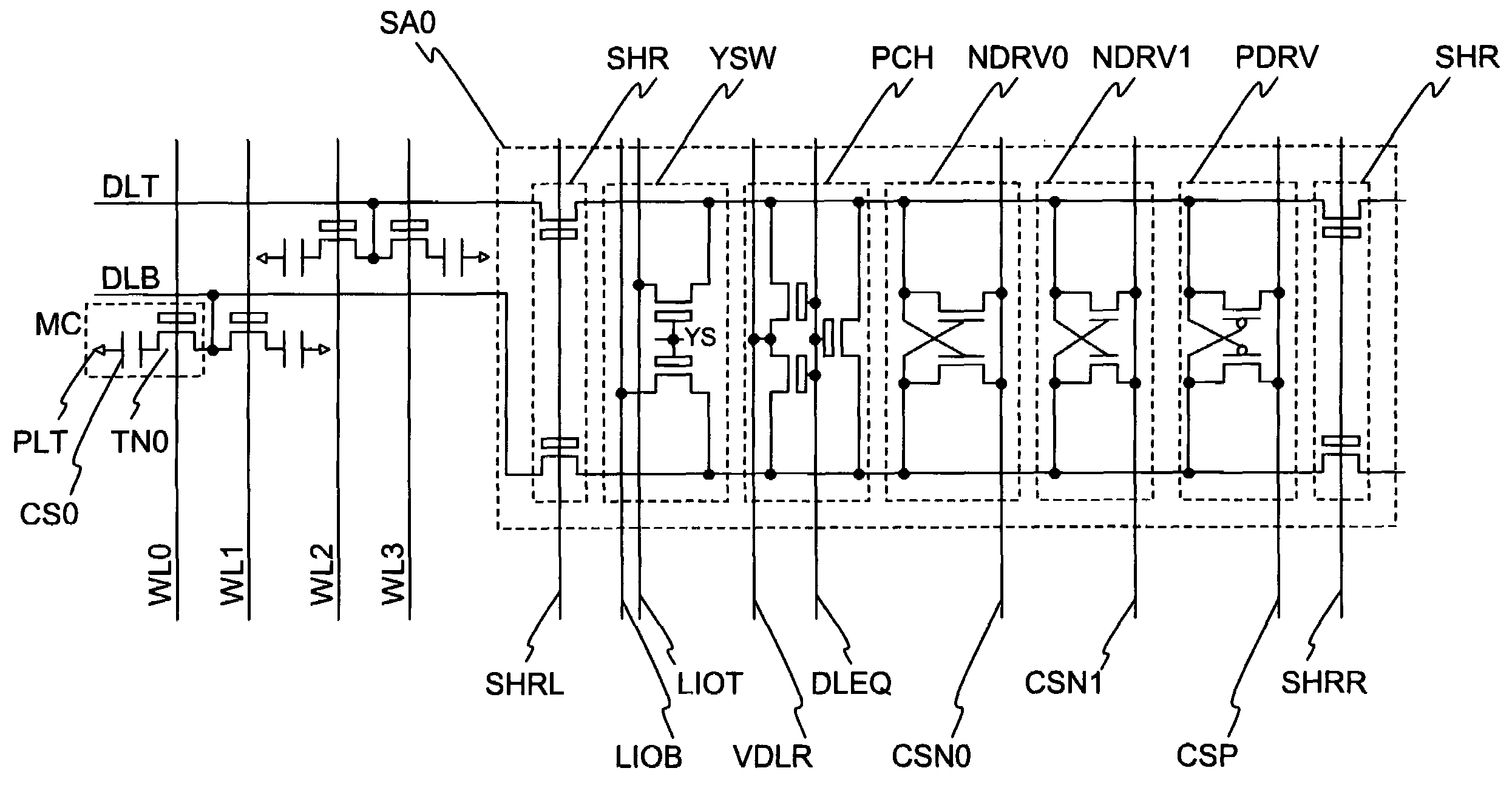
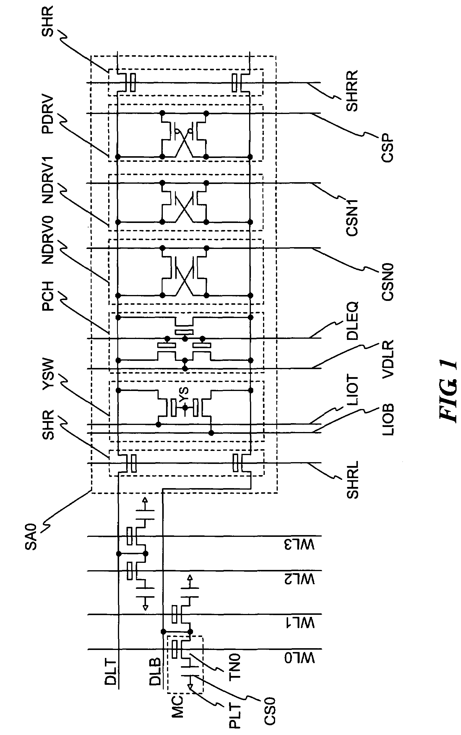
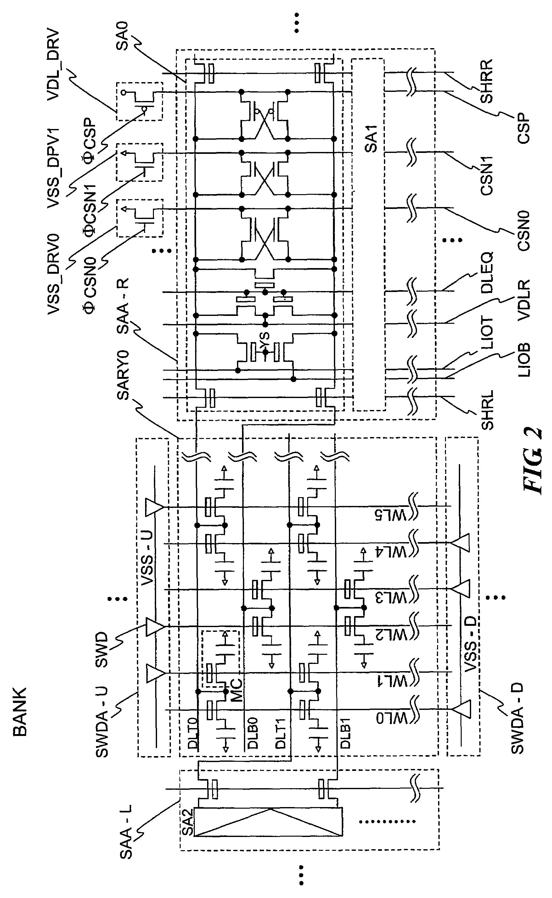
[0040]FIG. 1 shows the sense amplifier circuit SA0 comprised of a plurality of pull-down circuits NDRV0 and NDRV1, one pull-up circuit PDRV, a switch transistor SHR, a column switch YSW, and a precharge circuit PCH and a sub-array SARY0 comprised of a plurality of memory cells MC. Also, each of the reference symbols indicates common source lines CSN0 and CSN1 for driving the pull-down circuits NDRV0 and NDRV1, a common source line CSP for driving the pull-up circuit PDRV, a switch transistor drive lines SHRR and SHRL, a column switch drive line YS, a local data lines LIOT and LIOB, a precharge drive line DLEQ, precharge voltage VDLR, sub-word lines WL0 to WL3, data lines DLT and DLB, an access transistor TN0, a cell capacitor CS0, and a plate electrode PLT.

[0041]The plurality of memory cells MC are DRAM memory cells each provided with the N type channel MOS t...

second embodiment

(Second Embodiment)

[0061]The case where the ground voltage VSS is applied to the sub-word line WL of the memory cell MC at the time of non-selection has been described in the first embodiment. However, it is also possible to apply the negative voltage.

[0062]FIGS. 11 and 12 show the case where the negative word driver NSWD is applied to the sense amplifier circuit SA0 of this embodiment.

[0063]FIG. 11 shows a modified example of the sub-word driver SWD constituting the sub-word array SWDA-U and SWAD-D in FIG. 2. The symbols in FIG. 11 denote the word line voltage VPP, the negative word line voltage VKK, the main word line MWL, the sub-word line control signals FX and FXB, and the inverters INV0 and INV1. Since the control method of these signals is the same as that of the standard sub-word driver, the description thereof is omitted here.

[0064]FIG. 12 is a diagram showing the operation waveform in the case where the negative sub-word driver NSWD in FIG. 11 is applied to the sense ampli...

third embodiment

(Third Embodiment)

[0066]The case where a plurality of pull-down circuits are applied has been described in the first and second embodiments. In this case, the size of the offset of the pull-down circuit determines whether the stable read operation is enabled or the malfunction occurs. Therefore, since it is unnecessary to reduce the offset of the pull-up circuit more than necessary, the number of masks required to form the PMOS transistor can be reduced by using the so-called buried channel type PMOS transistor.

[0067]Of course, the present invention is not limited to the embodiments described above, and it is also preferable to form the sense amplifier circuit SA0 by using a plurality of pull-up circuits. In this case, it is preferable that the so-called dual gate transistor instead of the so-called buried channel type transistor is used as the PMOS transistor constituting the pull-up circuit. By doing so, though the number of masks required to form the PMOS transistor is increased,...


PUM


Abstract

A sense amplifier is constructed to reduce the occurrence of malfunctions in a memory read operation, and thus degraded chip yield, due to increased offset of the sense amplifier with further sealing down. The sense amplifier circuit is constructed with a plurality of pull-down circuits and a pull-up circuit, and a transistor in one of the plurality of pull-down circuits has a constant such as a channel length or a channel width larger than that of a transistor in another pulldown circuit. The pull-down circuit with a larger constant of a transistor is first activated, and then, the other pull-down circuit and the pull-up circuit are activated to perform the read operation.

Description

CROSS-REFERENCE TO RELATED APPLICATION[0001]The present application claims priority from Japanese Patent Application JP 2004-109598 filed on Apr. 2, 2004, the content of which is hereby incorporated by reference into this application.TECHNICAL FIELD OF THE INVENTION[0002]The present invention relates to a semiconductor memory device. More particularly, the present invention relates to a low power consumption, high-speed, and highly integrated semiconductor memory device and to a differential amplification operation of a semiconductor device in which a logic circuit and a semiconductor memory device are integrated.BACKGROUND OF THE INVENTION[0003]The dynamic random access memory (hereinafter, referred to as DRAM) which is one example of the semiconductor memory device is mounted in various types of electronic equipment used in our daily life, for example, in a main memory of a large-scale computer and a personal computer and a work memory of digital electronics such as a cellular pho...

Claims


Application Information

Patent Timeline
Patent Type & Authority Patents(United States)
IPC IPC(8): G11C7/02H01L21/8242G11C7/06G11C11/401G11C11/409G11C11/4091H01L27/108
CPCG11C7/065G11C11/4091G11C2207/065H01L27/10897H10B12/50A61G17/047
Inventor AKIYAMA, SATORUTAKEMURA, RIICHIROKAWAHARA, TAKAYUKISEKIGUCHI, TOMONORI
Owner HITACHI LTD
Why Eureka
Try Eureka