Solid-state imaging device and method of manufacturing the same

a solid-state imaging and modulation-type technology, applied in the direction of transistors, television systems, radio control devices, etc., can solve the problems of difficult to precisely align resist masks to gate electrodes, difficult to form resist mask openings, and increase noise in output image signals, so as to achieve the effect of precise positioning of the high impurity density region

Active Publication Date: 2007-06-12
INNOTECH CORP
View PDF3 Cites 8 Cited by
  • Summary
  • Abstract
  • Description
  • Claims
  • Application Information

AI Technical Summary

Benefits of technology

[0009]An object of the present invention is to provide a solid-state imaging device that is capable of forming carrier pockets (high impurity density region) easily and precisely.
[0021]According to the present invention, since the high impurity density region in the photo-detecting transistor is formed by self-alignment, the position of the high impurity density region becomes more precise. Moreover, since adjacent unit pixels have the impurity region in common and the drain regions of all unit pixels are connected to one another via the regions of same conductive type, the pixel isolation region is not needed, and thus accumulation of unit pixels can be achieved.

Problems solved by technology

Smaller gate width makes it difficult to form resist masks having openings corresponding to the carrier pockets.
It is also difficult to align the resist masks to the gate electrodes precisely.
Such variation in the position of the carrier pocket changes the threshold voltage caused by the accumulated charges, so the noise in output image signal will increase.

Method used


Image

  • Solid-state imaging device and method of manufacturing the same
  • Solid-state imaging device and method of manufacturing the same
  • Solid-state imaging device and method of manufacturing the same

Examples


Embodiment Construction

[0041]The embodiment of the present invention is described in detail hereinafter with reference to the accompanying drawings.

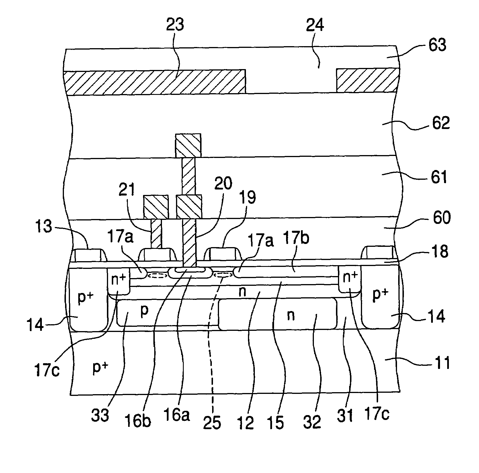
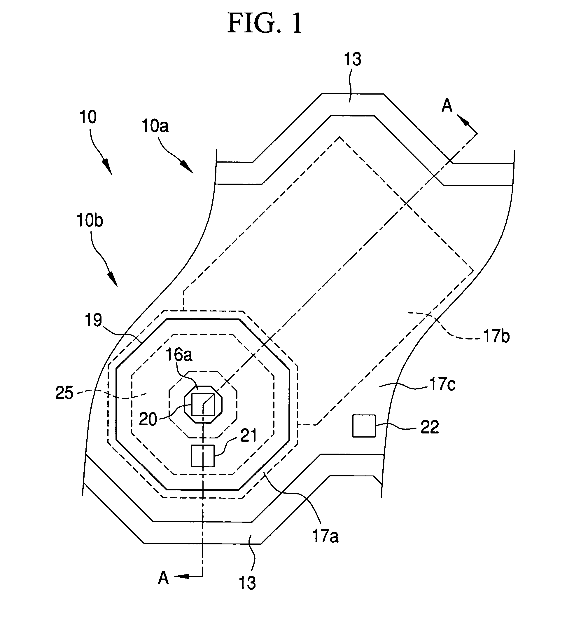
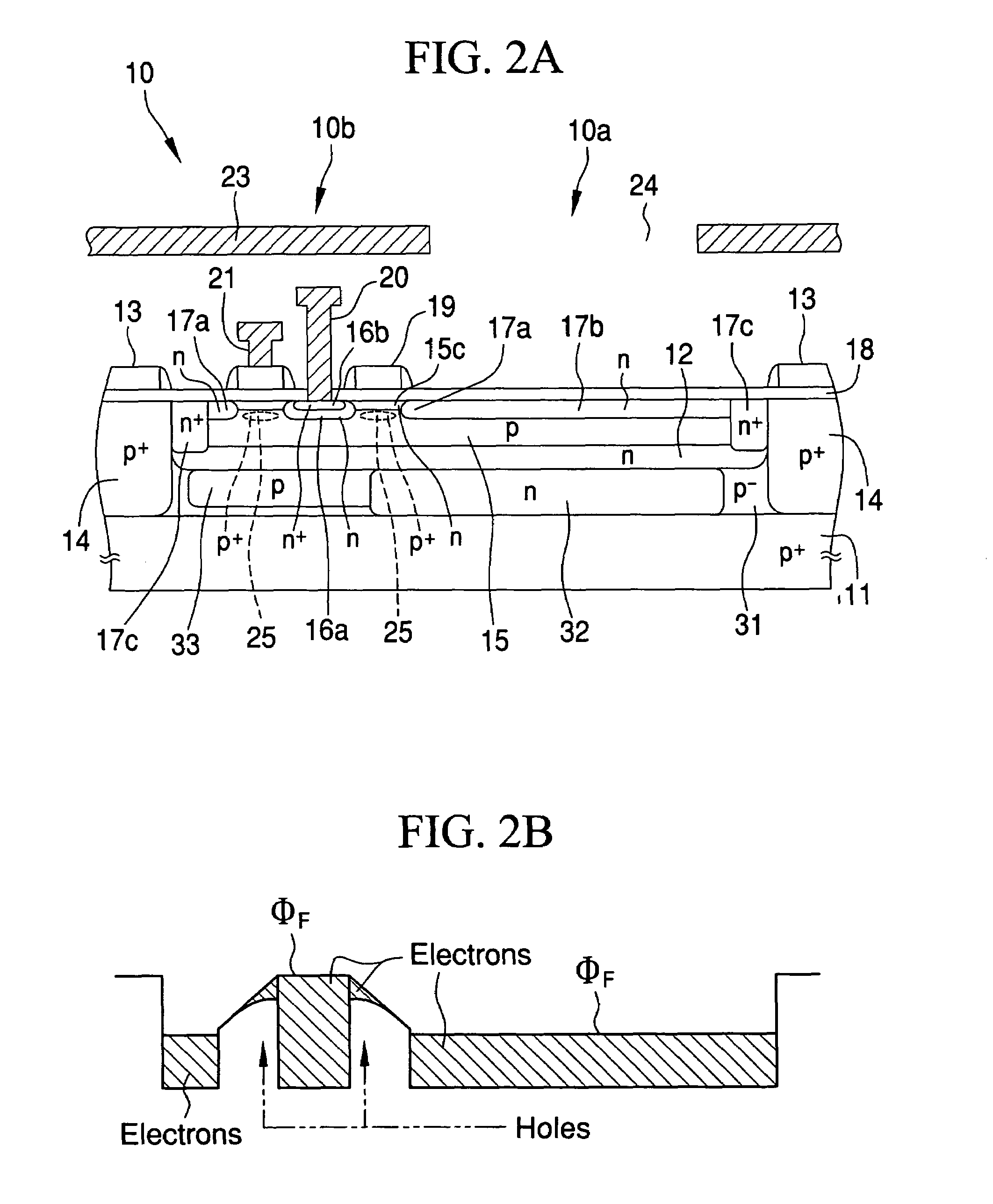
[0042]In FIGS. 1 and 2A that show a layout of a unit pixel of the solid-state imaging device, the unit pixel 10 includes a photo-diode 10a and a photo-signal detecting MOS transistor 10b that are adjacently provided in a p-type (opposite conductive type) well layer 15. The photo-diode 10a serves as an area to generate electron-hole pairs (photo-generated charges) by light illumination. The MOS transistor 10b is coupled to the photo-diode 10a, and the threshold voltage (source potential) thereof is modulated in accordance with the potential caused by the holes accumulated in a hole pocket 25. The hole pocket 25 is formed below the channel region of the MOS transistor 10b. The image signals are obtained by detecting the source potential.

[0043]A gate electrode 19 of the MOS transistor 10b has octagonal ring-shaped inner edge and outer edge. The gate electrode 19 ...


PUM


Abstract

The MOS type solid-state imaging device has plural pixels each of which comprises a photo-diode and a MOS transistor on a substrate. A gate electrode is formed on the channel dope layer formed in the surface of the p-type well layer. By ion implantation of n-type impurity ions via the gate electrode as the mask, the n-type source region and the drain region are formed in the region corresponding to the MOS transistor, and the n-type impurity region is also formed in the region corresponding to the photo-diode. In the well layer, a high impurity density region as a hole pocket is self-aligned to the gate electrode.

Description

[0001]This Non-provisional application claims priority under 35 U.S.C. § 119(a) on Patent Application No(s). 2003-145027 and 2003-415567 filed in Japan on May 22, 2003 and Dec. 12, 2003, the entire contents of which are hereby incorporated by reference.BACKGROUND OF THE INVENTION[0002]1. Field of the Invention[0003]The present invention relates to a threshold modulation type solid-state imaging device for use in video cameras, digital cameras, scanners, camera-equipped mobile phones, or the like, and to a method of manufacturing such solid-state imaging device.[0004]2. Description of Related Art[0005]Solid-state imaging devices of charged coupled device (CCD) type and metal oxide silicon (MOS) type have been widely used in most image input devices due to excellent mass productivity using advanced fine patterning techniques. Especially, the MOS type solid-state imaging devices have gained a great deal of attention because of the advantages that MOS type solid-state imaging devices ha...

Claims


Application Information

Patent Timeline
Patent Type & Authority Patents(United States)
IPC IPC(8): H01L31/062H01L27/146H01L21/00H04N5/335H04N5/357H04N5/374
CPCH01L27/14612H01L27/14689H01L27/14603H01L27/1461H01L27/14623
Inventor KOMORI, HIROFUMI
Owner INNOTECH CORP
Why Eureka
Try Eureka