Low power silicon thermal sensors and microfluidic devices based on the use of porous sealed air cavity technology or microchannel technology

a microfluidic device and low-power technology, applied in fluid speed measurement, optical radiation measurement, optical light guide, etc., can solve the problems of difficult processing after membrane formation and important drawbacks, and achieve the effect of increasing device sensitivity and reducing power consumption

Inactive Publication Date: 2007-06-19
NASSIOPOULOU ANDROULA G +2
View PDF10 Cites 26 Cited by
  • Summary
  • Abstract
  • Description
  • Claims
  • Application Information

AI Technical Summary

Benefits of technology

[0007]It is also an object of the present invention to provide a thermal flow sensor based on the above method. This sensor is illustrated in FIG. 2. It is composed of a silicon substrate (1) on which a closed structure of a porous silicon membrane (2) with a cavity underneath (3) is formed locally by an electrochemical dissolution of silicon in an HF:ethanol solution after the appropriate deposition and patterning of a masking layer. Depending on the thickness of the porous layer and the depth of the cavity, the mask for porous silicon formation is either a resist layer, or silicon nitride or a bilayer of SiO2 and polycrystalline silicon. An ohmic contact (13) has been created on the back side of the silicon substrate prior to the electrochemical process. The active elements of the sensor are composed of a heater (4) and two thermopiles (6,7) on each side of the heater. The number of thermocouples in each thermopile depends on the needed sensitivity of the device. The hot contacts of the thermocouples (5) are on porous silicon and the cold contacts (10) are on the bulk crystalline silicon substrate (1). The required interconnections (11) and metal pads (12) are formed by aluminum deposition and patterning. A passivation layer may be also deposited on top of the thermal flow sensor, consisting of an insulating layer, for example silicon oxide, or silicon nitride or polyimide. An electrical isolation layer (14) is deposited on top of the silicon substrate (1) so as to assure the electrical isolation between the sensor elements and the substrate. The thermocouple material is p-type poly / Al or n-type / p-type poly. The first case limits the temperature of operation of the device at around 400° C., while the second permits operation at temperatures up to ˜900° C. The heater is composed of p-type polycrystalline silicon and it is maintained at constant power or constant temperature by using an external electronic circuit, which stabilizes the power or the temperature by providing a current feedback if the temperature changes. The device can also operate at constant current on the heater, but the use of constant power is better in the case of a high flow range. Indeed, under flow the resistor is instantly cooled down by the gas flow and this causes a slight change of its resistance, which gives a measurable effect to the thermopiles output at high flow. This effect is minimized if the resistance change is compensated by a slight change in the current, so as to keep the power consumption or the temperature on the heater constant.
[0009]The thermal isolation by porous silicon with a cavity underneath, compared to the use of a single porous silicon layer in contact with the substrate offers the advantage of reducing power consumption and increasing the sensitivity of the device. Simulations carried out using MBMCAD V.4.8 package by MICROPROSM showed that the improvement depends on porous layer thickness and air cavity depth. FIG. 3 shows the effect of porous layer thickness on the temperature of the heater for a cavity of 20 μm and a heat flux of 8.57×10⁶ W / m2 applied on a 530 μm long polysilicon heater of width 20 μm and thickness 0.5 μm. This corresponds to a supplied power of 71 mW. For comparison, the results of a compact structure, where there is no cavity but instead a 40 μm thick porous layer is added, are shown with a star in the same figure. FIG. 4 shows the temperature on the heater for a 5 μm thick porous membrane and a cavity of variable thickness underneath. A comparison between isolation by a 40 μm compact porous silicon structure and a structure with 20 μm porous silicon membrane on 20 μm cavity is shown in FIG. 5. The heater is located at the middle of the membrane.
[0010]It is also the object of the present patent to provide a technique based on the use of the porous silicon / cavity technology for the formation of a microchannel under the active elements of the device, which may be used as a flow channel, open on its two endpoints. Such a device is shown in FIG. 6. It consists of a silicon substrate (15) on which a microfluidic channel (16) sealed with a porous silicon layer (17), is formed. The said microfluidic channel has two openings, which serve as inlet (18) and outlet (19) of a fluid. A thin silicon dioxide layer (25) is deposited on top of the channel for electrical isolation. The active elements of the thermal flow device are composed of a polysilicon heater (20) and two polysilicon resistors (21, 22) on each side of the heater. The device is used to measure the micro-flow developed into the microchannel. The heater is kept at a certain temperature and the flow measurement is based on sensing the temperature difference induced by the fluid between the two polysilicon resistors (21, 22) lying on the left and right side of the heater (20) in the upstream and downstream of the flow. The heater and resistors are connected to aluminum pads (23) through aluminum interconnects (24). A passivation layer can be deposited on top of the sensor, consisting of silicon oxide or silicon nitride or polyimide. The main advantage of this technology is that microflows can be formed and measured. This technology also offers important advantages in the case of liquid flows, since the liquid will not be in contact with the active elements of the device and so there is no need for complicated passivation schemes. It also offers advantages in gas flow measurements if the gas is corrosive.

Problems solved by technology

However, there is an important drawback in the above techniques.
It is related to the fragility of the structures which makes any processing after membrane formation very difficult.

Method used


Image

  • Low power silicon thermal sensors and microfluidic devices based on the use of porous sealed air cavity technology or microchannel technology
  • Low power silicon thermal sensors and microfluidic devices based on the use of porous sealed air cavity technology or microchannel technology
  • Low power silicon thermal sensors and microfluidic devices based on the use of porous sealed air cavity technology or microchannel technology

Examples


example 1

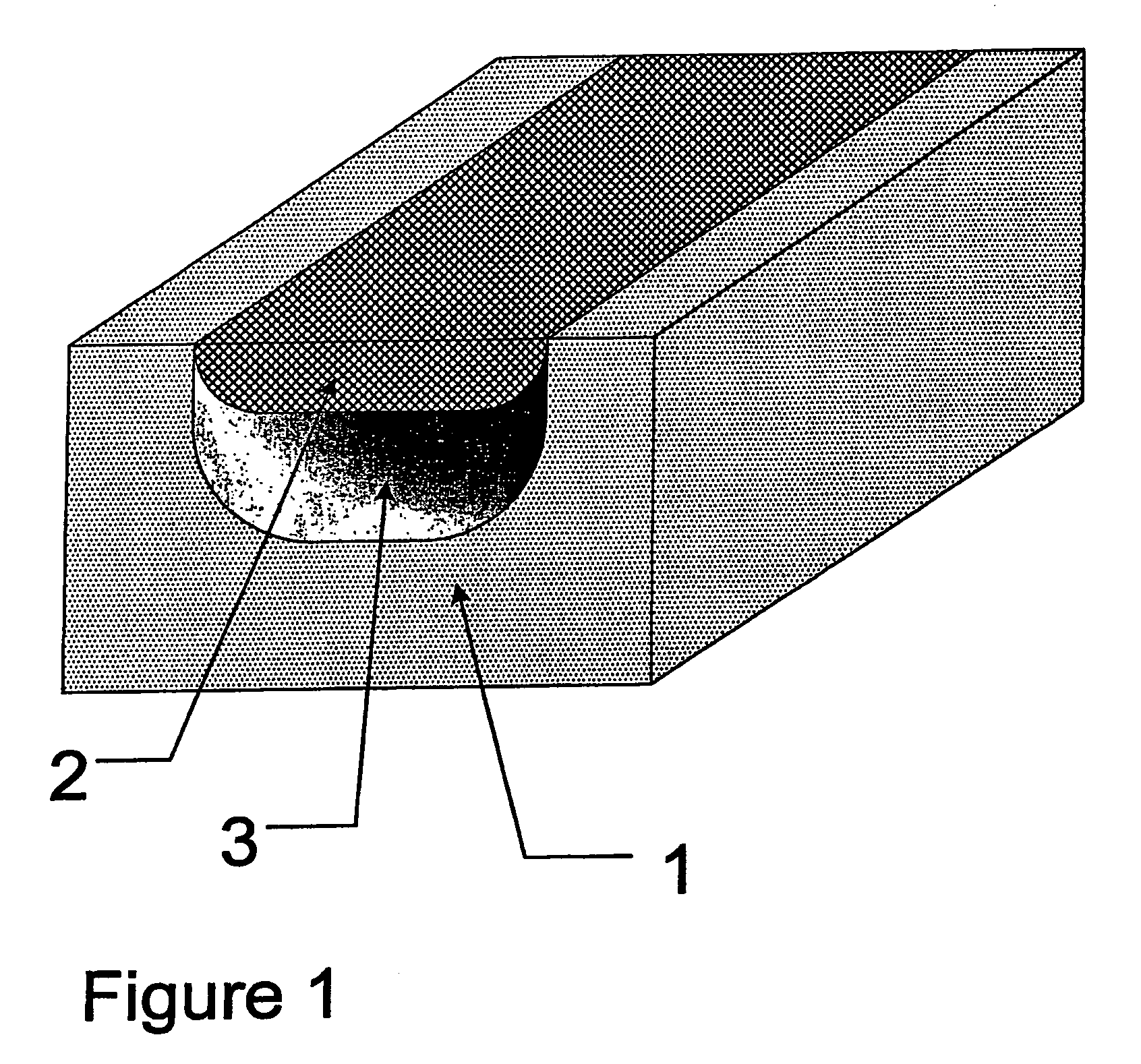
[0028]The process used for the formation of sealed or open microfluidic channels (3)(16) on a silicon substrate (1)(15). The porous silicon capping layer is planar with the silicon substrate. The process used is a combination of electrochemical dissolution and electropolishing of silicon by using a current density below (for porous silicon formation) or above (for electropolishing) a critical value. The fabrication process is the following: an ohmic contact (26) is first formed on the back side of the said silicon substrate (1)(15), used as anode in the electrochemical dissolution of silicon in order to form locally on silicon the porous silicon layer (2)(17). On the front side of the silicon substrate a masking layer for local porous silicon formation is then deposited and patterned. The porous silicon layer (2)(17) used as capping of the microchannel (3)(16) and the microchannel are formed in one electrochemical step by first using a current density below the critical value for el...

example 2

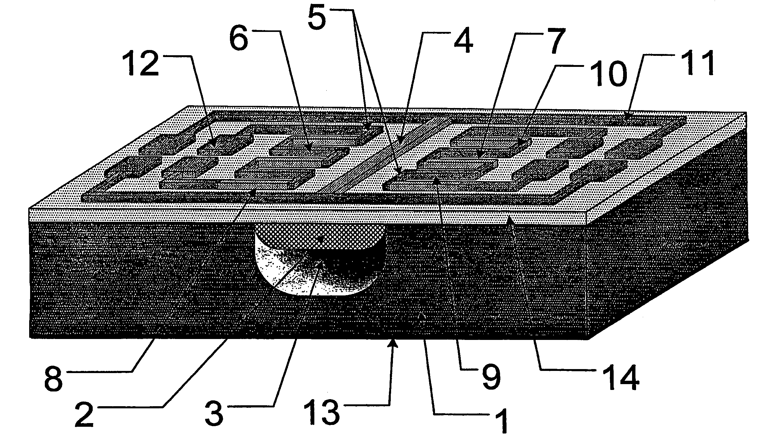
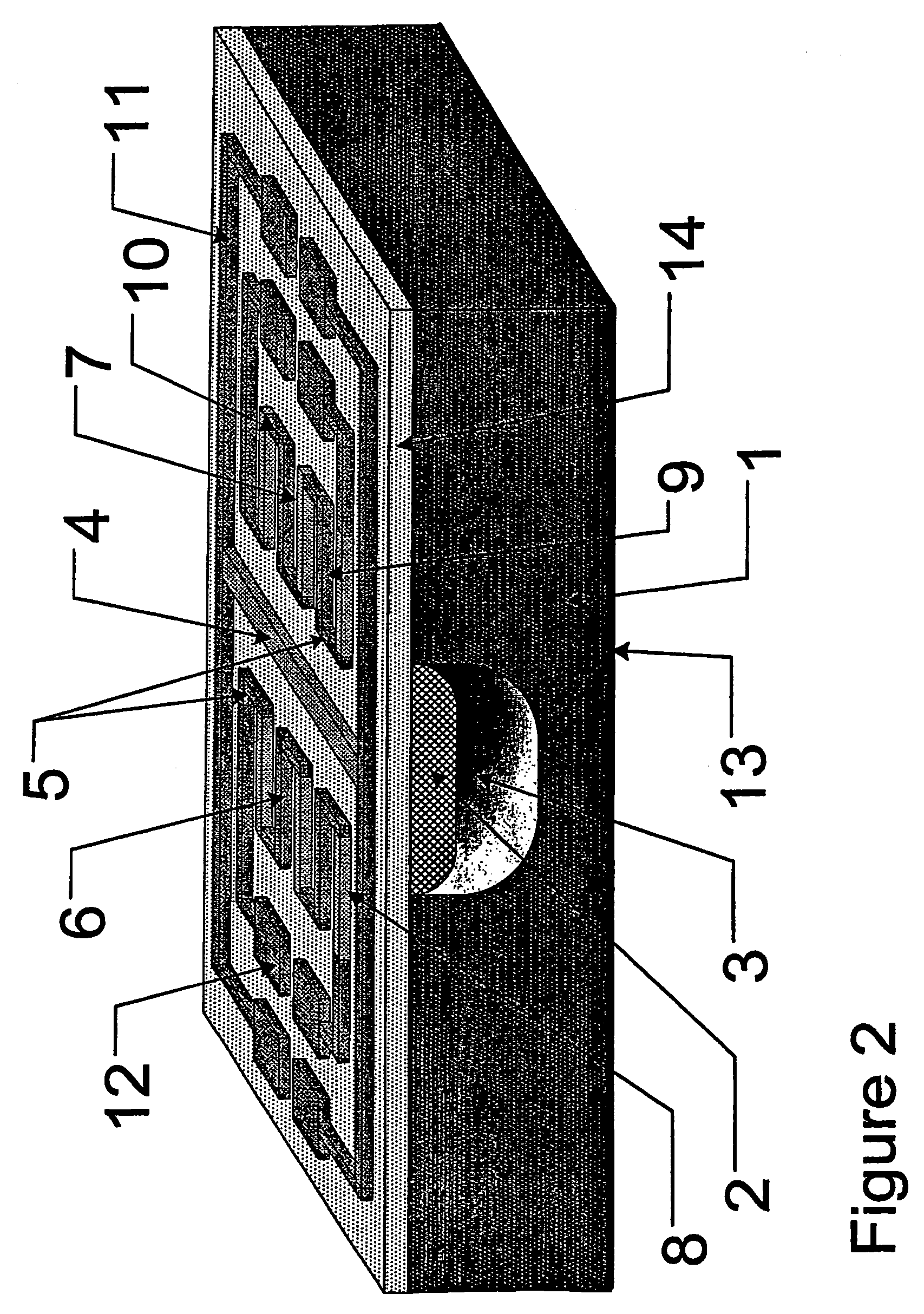
[0029]The fabrication process of a thermal flow sensor based on the process described in Example 1. It comprises the following steps: a) Creation of an ohmic contact (13) on the back side of the said silicon substrate (1), b) deposition and patterning of a masking layer for porous silicon formation in the front side of the silicon substrate, c) porous silicon (2) formation locally on the silicon substrate using electrochemical dissolution of bulk silicon. The current density used in the electrochemical process is below the value of the current density in the electropolishing regime, d) electrochemical dissolution of silicon under the porous silicon layer, using the electropolishing conditions, i.e. a current density above a critical value, so as to form a cavity (3) below a suspended porous silicon membrane (2), e) deposition of a thin dielectric layer for electrical isolation (14), f) deposition and patterning of polycrystalline silicon, which is then doped with p-type dopants, in ...

example 3

[0030]The fabrication process of a thermal microfluidic sensor based on the process described in Example 1. It comprises the following steps: a) creation of a microfluidic channel (16) sealed with a porous silicon layer (17) on the silicon substrate (15), b) deposition of a thin silicon dioxide layer (25) on top of the whole silicon substrate for electrical isolation, c) deposition and patterning of polycrystalline silicon in order to form a heater resistor (20) and two other resistors (21, 22) on its left and right sides, e) deposition and patterning of aluminum in order to form electrical interconnects (24) and metal pads (23) and f) opening of the inlet (18) and outlet (19) of the microchannel (16) by selectively etching locally the top silicon dioxide layer (25) and the silicon layer (15) underneath. On top of the flow sensor a passivation layer is deposited, consisting of silicon oxide or silicon nitride or polyimide.


PUM

PropertyMeasurementUnit
temperatureaaaaaaaaaa

Abstract

This invention provides a miniaturized silicon thermal flow sensor with improved characteristics, based on the use of two series of integrated thermocouples (6, 7) on each side of a heater (4), all integrated on a porous silicon membrane (2) on top of a cavity (3). Porous silicon (2) with the cavity (3) underneath provides very good thermal isolation for the sensor elements, so as the power needed to maintain the heater (4) at a given temperature is very low. The formation process of the porous silicon membrane (2) with the cavity (3) underneath is a two-step single electrochemical process. It is based on the fact that when the anodic current is relatively low, we are in a regime of porous silicon formation, while if this current exceeds a certain value we turn into a regime of electropolishing. The process starts at low current to form porous silicon (2) and it is then turned into electropolishing conditions to form the cavity (3) underneath. Various types of thermal sensor devices, such as flow sensors, gas sensors, IR detectors, humidity sensors and thermoelectric power generators are described using the proposed methodology. Furthermore the present invention provides a method for the formation of microfluidic channels (16) using the same technique of porous silicon (17) and cavity (16) formation.

Description

FIELD OF THE INVENTION[0001]This invention relates to low power silicon thermal sensors and microfluidic devices, which use a micromachining technique to fabricate electrochemically porous silicon membranes with a cavity underneath. In the case of thermal sensors the structure used is of the closed type (porous silicon membrane on top of a cavity), while in microfluidics the same technique is used to open microchannels with a porous silicon membrane on top.DESCRIPTION OF THE RELATED ART[0002]Silicon thermal flow sensors are based on heat exchange between the fluid and the hot parts of the device, which are kept at relatively high temperature, of the order of 100–180° C. In silicon thermal gas sensors, this temperature has, sometimes, to exceed 400° C. In order to keep the temperature constant, the electric power on the heater has to compensate thermal losses due to conduction, convection and radiation. Losses due to conduction through the substrate on which the active elements of th...

Claims


Application Information

Patent Timeline
Patent Type & Authority Patents(United States)
IPC IPC(8): G01J5/20H01L21/02H01L27/14H01L31/0248G01K13/02B81B1/00B81B3/00B81C1/00G01F1/684G01K7/01G01K7/02
CPCG01K7/028G01F1/6845B81C1/00071B81B2201/058B81B2203/0127B81B2203/0315B81C2201/0114B81C2201/0115
Inventor NASSIOPOULOU, ANDROULA G.KALTSAS, GRIGORISPAGONIS, DIMITRIOS N.
Owner NASSIOPOULOU ANDROULA G
Why Eureka
Try Eureka