[0030]According to a major
advantage of the invention, therefore, the dummy
cell having a structure and a form similar to those of the memory cell can be used for executing data reading corresponding to a comparison between passing currents of the
data lines connected to the memory cell and the dummy cell, respectively. Consequently,
special design and manufacturing steps are not required for manufacturing the dummy cell. Therefore, such a problem does not occur that complicated structures increase a
chip area and impair a
processing margin of the
memory array and others, and therefore an intended data read margin can be ensure by arranging the normal memory cells and dummy cells in the same
memory array.
[0031]According to another aspect of the invention, a thin film
magnetic memory device includes a plurality of memory cells, a dummy cell, a first
voltage line, a second voltage line, first and second data lines, and a data reading portion. Each of the plurality of memory cells is configured to exhibit an electric resistance corresponding to a
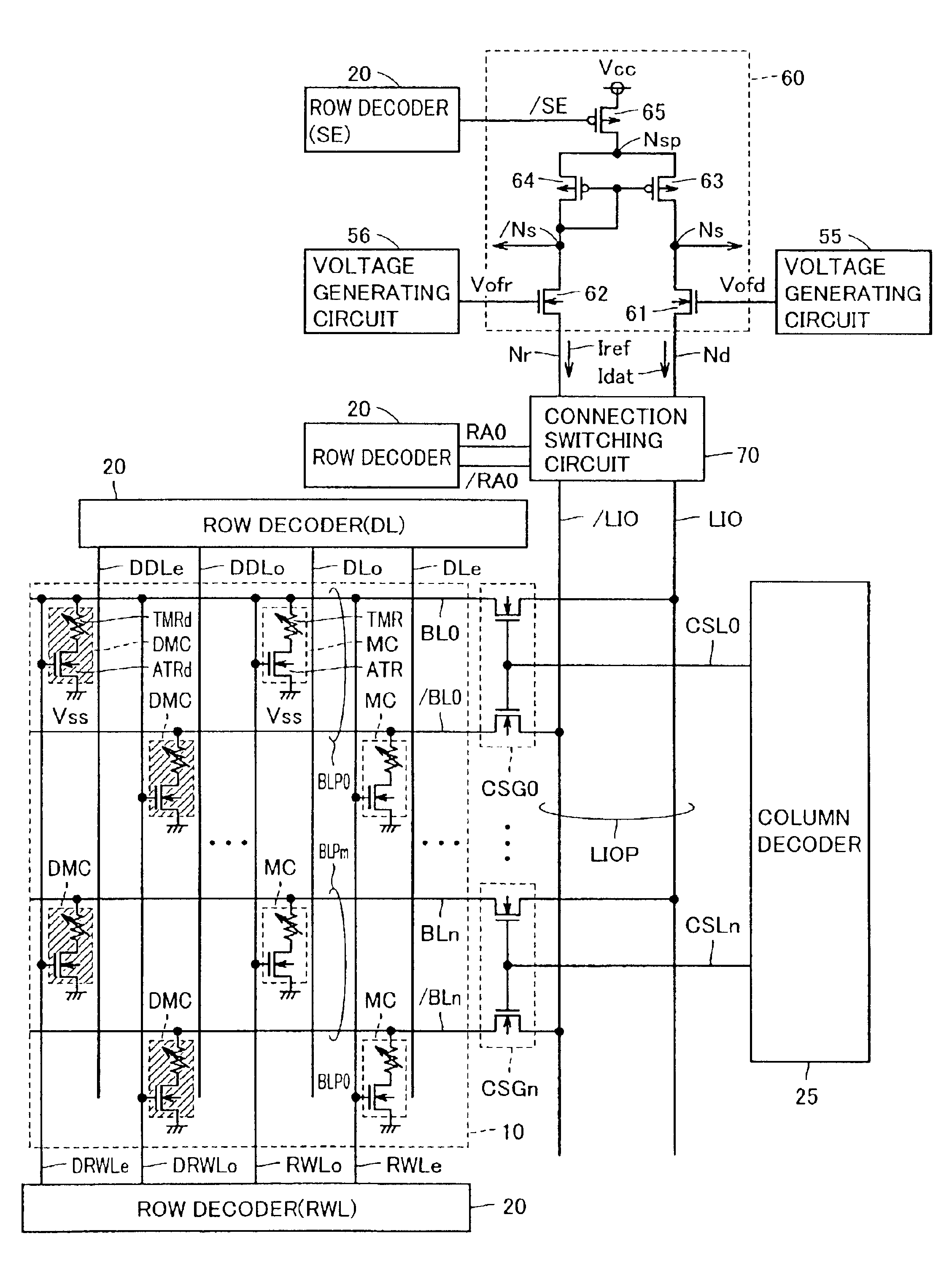
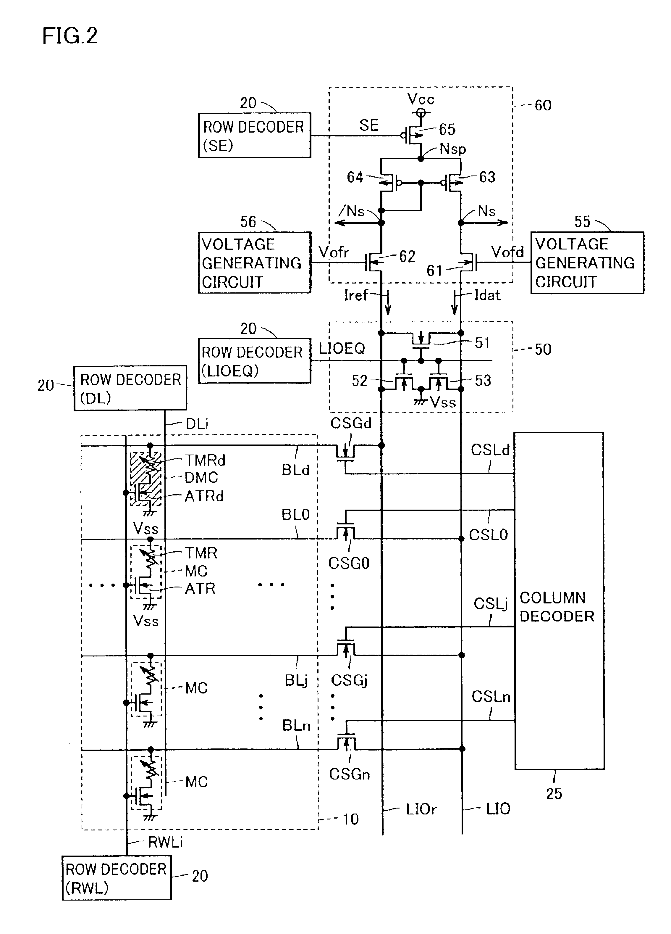
magnetization direction, and is magnetized in a direction corresponding to storage data. The dummy cell has a structure and a form similar to those of the memory cell, and is magnetized in advance in a direction corresponding to a predetermined level of the storage data. The first voltage line is provided for the plurality of memory cells for transmitting a first predetermined voltage. The second voltage line is provided corresponding to the dummy cell for transmitting a second predetermined voltage different from the first predetermined voltage. The first and second data lines are electrically coupled to the first and second voltage lines via the selected memory cell among the plurality of memory cells and the dummy cell in a data read operation, respectively. The data reading portion performs data reading in accordance with a difference between passing currents of the first and second data lines. The first and second predetermined voltages are determined such that the passing current of the dummy cell attains a level intermediate between two kinds of passing currents corresponding to respective levels of the storage data in the selected memory cell.
[0032]According to the thin film magnetic memory device, a structure for providing an offset between the passing currents of the selected memory cell and the dummy cell is not required in data read circuitry, and the data reading can be performed by using the dummy cell of the structure similar to that of the normal MTJ memory cell. Therefore,
special design and manufacturing steps are not required for producing the dummy cell so that it is possible to prevent increase in
chip area and impairing of a
processing margin of a memory array and others, which may be caused by complication of structures, and an intended data read margin can be ensured by arranging the normal memory cells and the dummy cell in the same memory array. Further, a structure of a data read circuit
system can be simple.
[0033]According to still another aspect of the invention, a thin film magnetic memory device includes a plurality of memory cells, a dummy cell, first and second data lines, and a data reading portion. Each of the plurality of memory cells has a
magneto-resistance element configured to be magnetized in a direction corresponding to a level of storage data, and to have either a first or second electric resistance in accordance with the
magnetization direction, and an access
transistor connected in series to the
magneto-resistance element and being selectively turned on in a data read operation. The dummy cell is provided for comparing a passing current with that of the selected memory cell selected as an access target among the plurality of memory cells in the data read operation. The first and second data lines are electrically coupled to a fixed voltage via the selected memory cell and the dummy cell in the data read operation, respectively. The data reading portion performs data reading in accordance with a difference between passing currents of the first and second data lines. The dummy cell includes a dummy
magneto-resistance element having a structure and a form similar to those of the magneto-resistance element and being magnetized in advance to have a smaller one between the first and second electric resistances, a dummy access
transistor connected in series to the dummy magneto-resistance element, being selectively turned on in the data read operation and being designed similarly to the access
transistor, and a dummy resistance adding portion connected in series to the dummy magneto-resistance element, and having an electric resistance smaller than a difference between the first and second electric resistances. The dummy resistance adding portion has at least one transistor designed similarly to the access transistor and having a gate supplied with an adjustable control voltage.
[0034]According to the thin film magnetic memory device described above, since the transistor and the dummy access element forming the dummy resistance adding portion are designed to have sizes similar to those of the access element, the dummy cells can be arranged efficiently in accordance with an arrangement
pitch of the memory cells. The memory cells and dummy cell are arranged continuously so that lowering of the processing margin of the memory array can be avoided.
[0035]According to yet another aspect of the invention, a thin film magnetic memory device includes a memory array, a first voltage line, a second voltage line, a dummy resistance adding portion, first and second data lines, and a data reading portion. The memory array is provided with a plurality of memory cells and a dummy cell for comparing a passing current with that of the selected memory cell selected as an access target among the plurality of memory cells in a data read operation. Each memory cell includes a magneto-resistance element configured to be magnetized in a direction corresponding to a level of storage data and to have either a first or second electric resistance in accordance with the
magnetization direction, and an access transistor connected in series to the magneto-resistance element and being selectively turned on in the data read operation. The dummy cell includes a dummy magneto-resistance element having a structure and a form similar to those of the magneto-resistance element, and being magnetized in advance to have fixedly smaller one between the first and second electric resistances, and a dummy access transistor connected in series to the dummy magneto-resistance element, being selectively turned on in the data read operation and being designed similarly to the access transistor. The first voltage line is provided corresponding to the plurality of memory cells for transmitting a fixed voltage. The second voltage line is provided corresponding to the dummy cell for transmitting the fixed voltage. The first and second data lines are electrically coupled to the first and second voltage lines via the selected memory cell and the dummy cell in the data read operation, respectively. The data reading portion performs data reading in accordance with a difference between passing currents of the first and second data lines. The dummy resistance adding portion is located outside the memory array, is connected in series to the second voltage line and has an electric resistance smaller than a difference between the first and second electric resistances.

