Energy conversion and storage films and devices by physical vapor deposition of titanium and titanium oxides and sub-oxides

a technology of energy conversion and storage films and devices, applied in vacuum evaporation coatings, sputtering coatings, coatings, etc., can solve the problems of poor insulation properties, difficult amorphous titania deposited, and not utilized commercially for titanium oxide layers

Inactive Publication Date: 2007-07-03
DEMARAY
View PDF256 Cites 63 Cited by
  • Summary
  • Abstract
  • Description
  • Claims
  • Application Information

AI Technical Summary

Problems solved by technology

Currently, titanium oxide layers are not utilized commercially in energy storage, charge storage, or energy conversion systems because such layers are difficult to deposit, difficult to etch, are known to have large concentrations of defects, and have poor insulation properties due to a propensity for oxygen deficiency and the diffusion of oxygen defects in the layers.
Additionally, amorphous titania is difficult to deposit due to its low recrystalization temperature (about 250° C.
However, these materials have not found utilization because of their difficult manufacture in films and their susceptibility to oxidation.
Ti4O7, however, is also difficult to fabricate, especially in thin film form.
Additional to the difficulty of fabricating titanium oxide or sub oxide materials in useful thin film form, it also has proven difficult to dope these materials with, for example, rare earth ions, in useful or uniform concentration.
Therefore, utilization of titanium oxide and suboxide films, with or without rare earth doping, has been significantly limited by previously available thin film processes.
Capacitive density of 10,000 to 12,000 pico Farads / mm2 is very difficult to achieve with present conductors and dielectrics.

Method used


Image

  • Energy conversion and storage films and devices by physical vapor deposition of titanium and titanium oxides and sub-oxides
  • Energy conversion and storage films and devices by physical vapor deposition of titanium and titanium oxides and sub-oxides
  • Energy conversion and storage films and devices by physical vapor deposition of titanium and titanium oxides and sub-oxides

Examples


example 1

Deposition of Ti4O7 Film

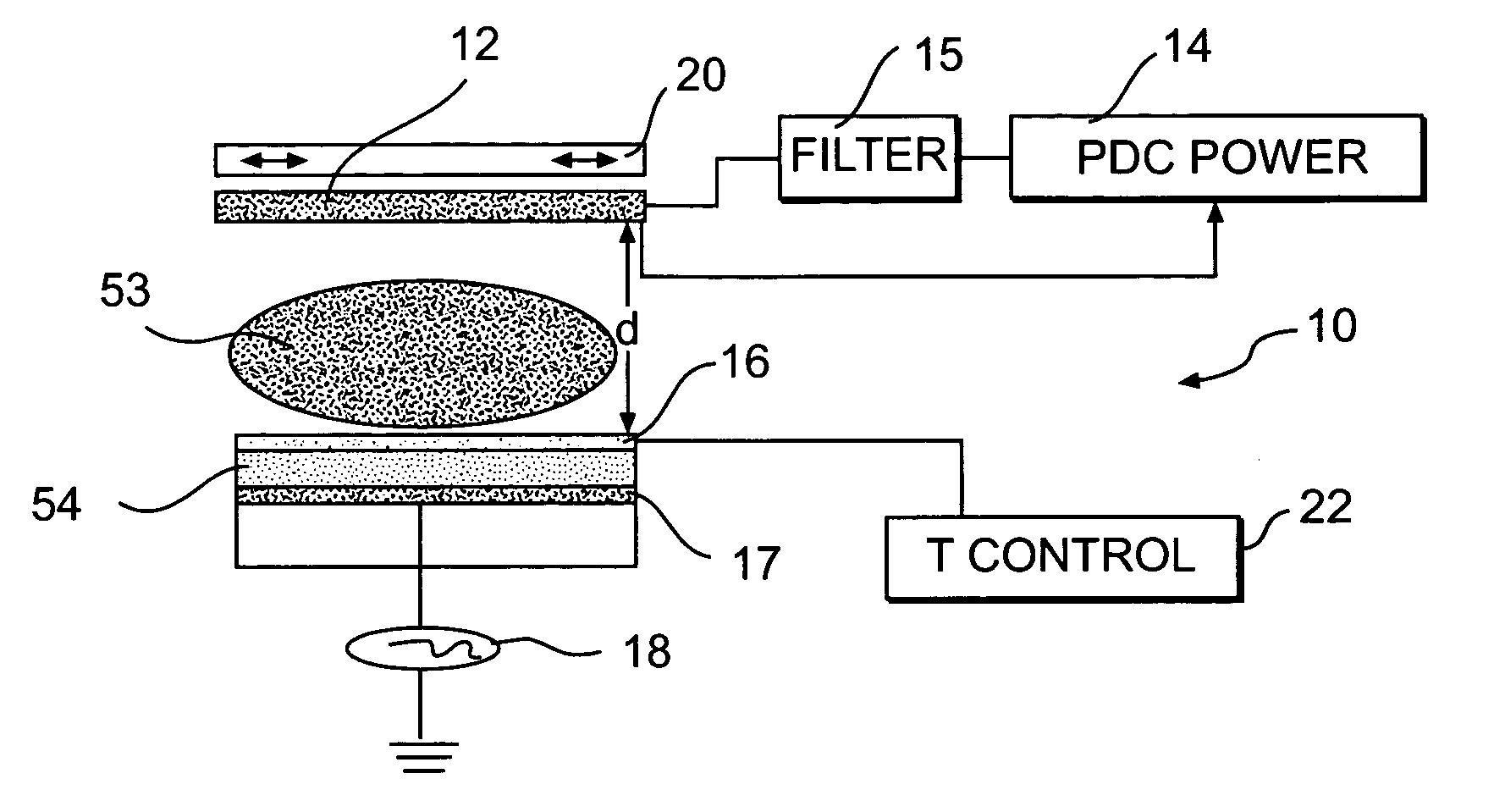
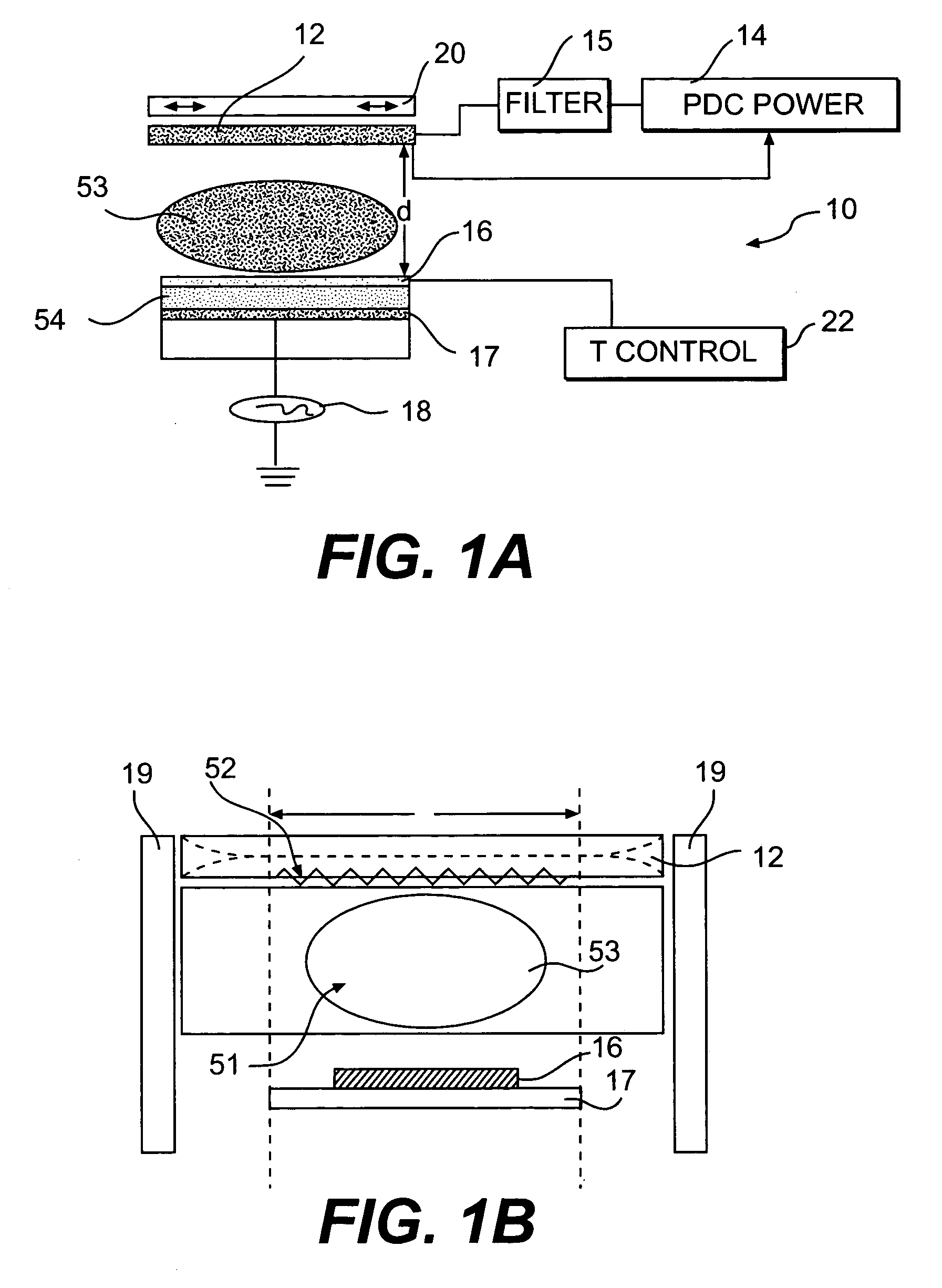
[0068]In this example, Ti4O7 films were deposited using a Pulse DC scanning magnetron PVD process as was previously described in U.S. application Ser. No. 10 / 101,341. The target was a about 1 mm thick, about 16.5×12.5 mm2 tiles of titanium oxide target obtained from a sheet of Ebonex™ which compounded of bulk Ti4O7 was bonded onto a backing plate. Ebonex™ can be obtained from Atraverda Ltd., Oakham Business Park, Mansfield, UK. A pulsed DC generator from Advanced Energy (Pinnacle Plus) was used as the target power supply. The pulsing frequency can be varied from 0-350 KHz. Reversed duty cycle can be varied from 1.3 μs to 5 μs depending on the pulsing frequency. Target power was fixed at 2 KW and pulsing frequency was 200 KHz during deposition, Ar flow rate is 100 sccm. The deposition rate at this condition is 14 Å / sec over a 40 by 50 cm substrate 101. A 100 W at 2 MHz bias was supplied to the substrate. The bias power supply can be an RF supply produced by EN...

example 2

Deposition of TiO2 on Ti—Ti4O7 Film Stack

[0070]In this example, TiO2 films were deposited using a 2 MHz RF biased, Pulse DC scanning magnetron PVD process as was previously described in U.S. application Ser. No. 10 / 101,341. The substrate size can be up to 600×720 mm2. The target was a ˜7 mm thick, ˜630×750 mm2 Ti plate of 99.9% purity. A pulsed DC generator, or PDC power supply from Advanced Energy (Pinnacle Plus) was used as the target power supply. The pulsing frequency can be varied from 0-350 KHz. Reversed duty cycle can be varied from 1.3 μs to 5 μs depending on the pulsing frequency. An ENI RF generator and ENI Impedance matching unit were used for the substrate bias. A 100 W with a 2 MHz RF generator, which can be an EFI supply, was utilized. The chamber base pressure was kept below 2×10⁻⁷ Torr. The substrate temperature was below 200° C. during deposition.

[0071]A systematic DOE (design of experiments) were carried out on both n++ type bare Si wafers and Al metallized wafers....

example 3

Deposition of TiO2 on Ti—TiOx (x<2) Film Stack

[0075]A layer of TiO2 was deposited on a titanium coated substrate. About 2000 Å of Ti metal was deposited at 7 KW of PDC target power, with Ar flow of 100 sccm and bias power of 200 W. After Ti deposition, TiO2 was deposited in the same chamber without-oxide burn in. This process resulted in a Ti—TiOy—TiO2 (y<2) film stack. The k value of a 200 Å film was as high as 60.

[0076]FIGS. 9A and 9B illustrate an SEM cross-section of a Ti4O7 Ebonex™ target (FIG. 9A) and an SEM cross section of the Ti4O6.8 layer (FIG. 9B) deposited from the Ebonex™ target according to the present invention. The deposited film shows smooth deposition of the layer. The Ebonex™ target shown in FIG. 9A shows an open porousity material with high roughness. The deposited layer shown in FIG. 9B, however, shows a highly dense layer with a smooth surface condition.

[0077]Table I shows the effects of the dielectric properties of TiO2 deposited according the present inventio...


PUM

PropertyMeasurementUnit
dielectric constantaaaaaaaaaa
sizeaaaaaaaaaa
sizeaaaaaaaaaa

Abstract

High density oxide films are deposited by a pulsed-DC, biased, reactive sputtering process from a titanium containing target to form high quality titanium containing oxide films. A method of forming a titanium based layer or film according to the present invention includes depositing a layer of titanium containing oxide by pulsed-DC, biased reactive sputtering process on a substrate. In some embodiments, the layer is TiO2. In some embodiments, the layer is a sub-oxide of Titanium. In some embodiments, the layer is TixOy wherein x is between about 1 and about 4 and y is between about 1 and about 7. In some embodiments, the layer can be doped with one or more rare-earth ions. Such layers are useful in energy and charge storage, and energy conversion technologies.

Description

RELATED APPLICATIONS[0001]The present invention claims priority to U.S. Provisional Application Ser. No. 60 / 473,375, “Energy Conversion and Storage Devices by Physical Vapor Deposition of Titanium Oxides and Sub-Oxides,” by Richard E. Demaray and Hong Mei Zhang, filed on May 23, 2003, herein incorporated by reference in its entirety.BACKGROUND[0002]1. Field of the Invention[0003]The present invention is related to fabrication of thin films for planar energy and charge storage and energy conversion and, in particular, thin films deposited of titanium and titanium oxides, sub oxides, and rare earth doped titanium oxides and sub oxides for planar energy and charge storage and energy conversion.[0004]2. Discussion of Related Art[0005]Currently, titanium oxide layers are not utilized commercially in energy storage, charge storage, or energy conversion systems because such layers are difficult to deposit, difficult to etch, are known to have large concentrations of defects, and have poor ...

Claims


Application Information

Patent Timeline
Patent Type & Authority Patents(United States)
IPC IPC(8): H01L21/31H01L21/469C23C14/00C23C14/08C23C14/34H01L21/285H01L21/314H01L21/316H01L21/768
CPCC23C14/0036C23C14/083C23C14/345H01L21/2855H01L21/31604H01L21/7687H01L21/02266H01L21/02192H01L21/02194H01L21/02186
Inventor DEMARAY, RICHARD E.ZHANG, HONG MEINARASIMHAN, MUKUNDANMILONOPOULOU, VASSILIKI
Owner DEMARAY
Why Eureka
Try Eureka