Nitrogen-containing field effect transistor gate stack containing a threshold voltage control layer formed via deposition of a metal oxide

a technology of metal oxide and gate stack, which is applied in the direction of semiconductor devices, semiconductor/solid-state device details, electrical apparatus, etc., can solve the problems of affecting the stability of the threshold voltage and the and it is nearly impossible to develop a cmos technology capable of stabilizing the threshold voltage and flatband voltage of the fet. achieve the effect o

Inactive Publication Date: 2007-07-10
GLOBALFOUNDRIES INC
View PDF10 Cites 51 Cited by
  • Summary
  • Abstract
  • Description
  • Claims
  • Application Information

AI Technical Summary

Benefits of technology

[0010]The present invention solves the above problem of threshold and flatband voltage shift by providing a Vt stabilization layer between a gate dielectric and a gate electrode. The Vt stabilization layer employed in the present invention is capable of preventing interaction between the gate dielectric and the gate electrode by spatial separation. Moreover, the Vt stabilization layer employed in the present invention has a sufficiently high dielectric constant (on the order of about 4.0 or greater) such that there is a minimal decrease in gate capacitance (due to series capacitance effect) with its addition. The Vt stabilization layer employed in the present invention may dissociate, at least partially, to provide a supply of p-type dopants in the near interfacial layer to ensure p-type behavior of the near interfacial gate electrode and it can prevent outdiffusion of impurities from the gate dielectric into the gate electrode and vice versa.
[0011]Another characteristic feature of the inventive Vt stabilization layer is that it is chemically stable so that silicon cannot reduce it. In cases in which some dissociation of the inventive Vt stabilization layer may occur, the inventive Vt stabilization layer should not be an n-type dopant to silicon. Rather, the inventive Vt stabilization layer can be either a p-type dopant or a neutral dopant so that device performance is not adversely affected. Also, the Vt stabilization layer employed in the present invention should be a refractory compound that is able to withstand high temperatures (of approximately 1000° C., typical of standard CMOS processing).
[0018]In one highly preferred embodiment of the present invention, a CMOS structure is provided that includes a semiconductor substrate having source and drain diffusion regions located therein, said source and drain diffusion regions are separated by a device channel; and a gate stack located on top of said device channel, said gate stack comprising a hafnium-containing high k gate dielectric, a nitrided aluminum oxide Vt stabilization layer and a gate electrode, said nitrided aluminum oxide Vt stabilization layer is located between said hafnium-containing high k gate dielectric and said gate electrode and is capable of stabilizing the structure's threshold voltage and flatband voltage to a targeted value.
[0019]In another aspect of the present invention, a method of forming a complementary metal oxide semiconductor (CMOS) structure having improved threshold voltage and flatband voltage stability is provided. The method includes the steps of providing a gate stack comprising a gate dielectric, a Vt stabilization layer and a gate electrode on a semiconductor substrate, said Vt stabilization layer is located between said gate dielectric and said gate electrode and comprises a nitrided metal oxide, or a nitrogen-free metal oxide, with the proviso that when the Vt stabilization layer comprises a nitrogen-free metal oxide, at least one of the semiconductor substrate or the gate dielectric includes nitrogen; and applying a bias by any known technique to said gate stack, whereby said Vt stabilization layer stabilizes the structure's threshold voltage and flatband voltage to a targeted value.

Problems solved by technology

Unfortunately, when p-type field effect transistors are fabricated using a dielectric such as hafnium oxide or hafnium silicate, it is a well known problem that the flatband voltage of the device is shifted from its ideal position of close to about +1 V, to about 0 + / −300 mV.
Although substrate engineering is one possible means to stabilize threshold voltage shift, it can do so to a limited extent, which is inadequate for FETs that include a gate stack comprising a poly-Si gate electrode and a hafnium-containing high dielectric constant gate dielectric.
In view of the above mentioned problem in threshold voltage and flatband voltage shift, it has been nearly impossible to develop a CMOS technology that is capable of stabilizing the threshold voltage and flatband voltage for such FETs.

Method used


Image

  • Nitrogen-containing field effect transistor gate stack containing a threshold voltage control layer formed via deposition of a metal oxide
  • Nitrogen-containing field effect transistor gate stack containing a threshold voltage control layer formed via deposition of a metal oxide
  • Nitrogen-containing field effect transistor gate stack containing a threshold voltage control layer formed via deposition of a metal oxide

Examples


Embodiment Construction

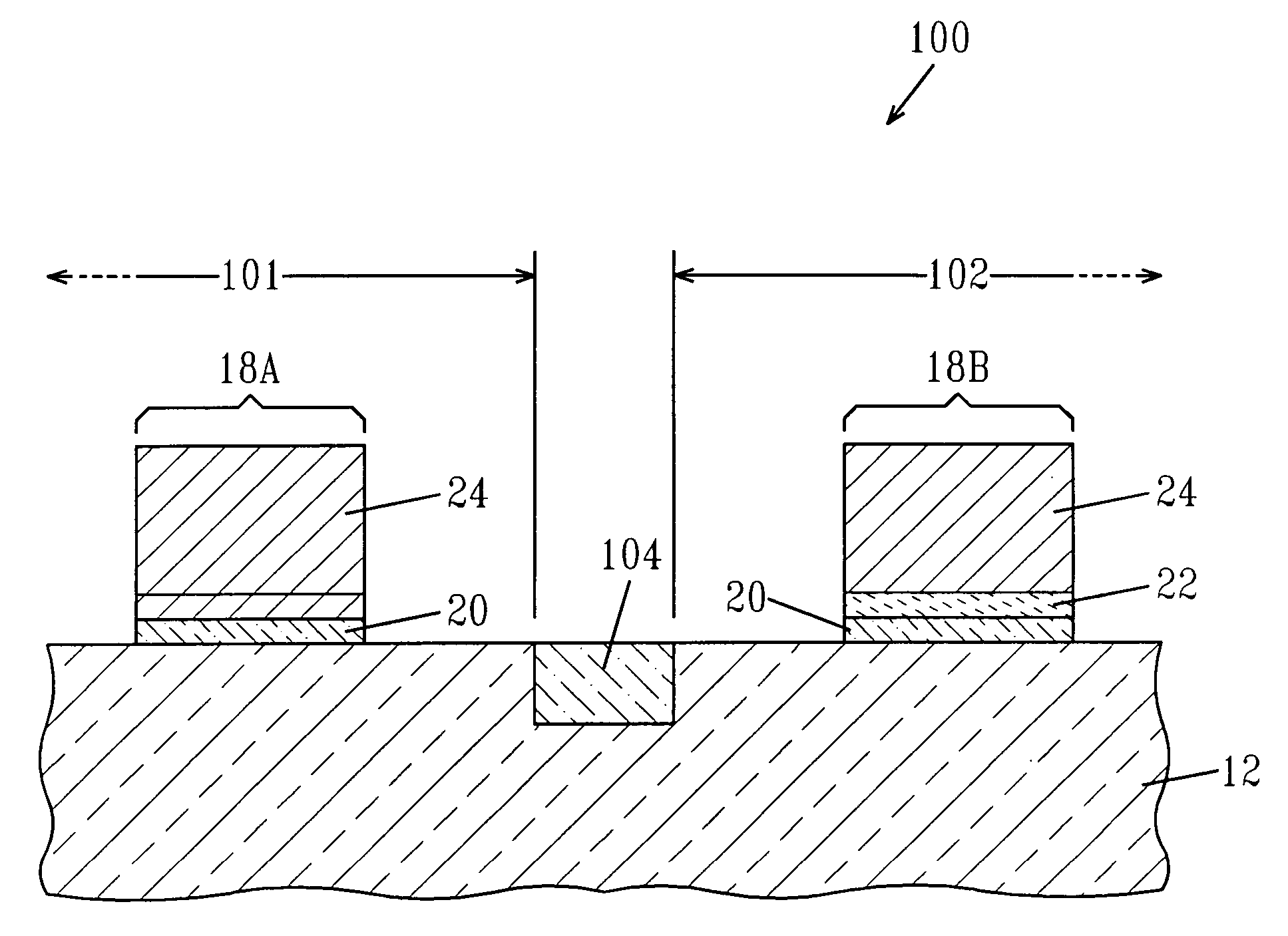
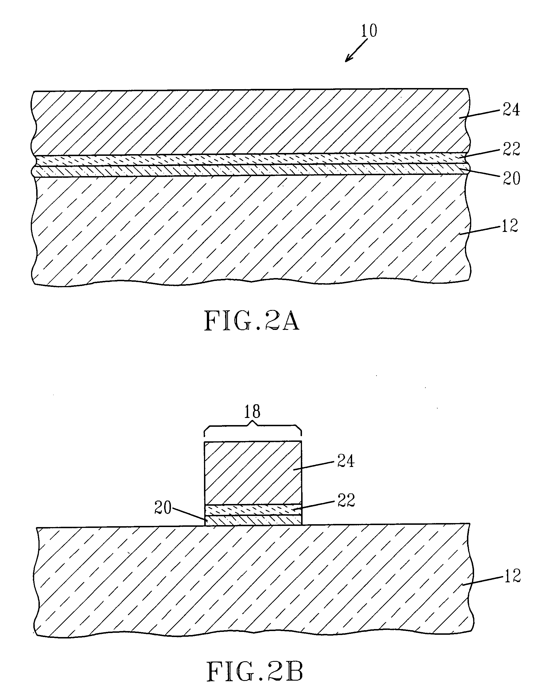
[0023]The present invention, which provides a CMOS structure that includes a Vt stabilization layer between a gate electrode and a gate dielectric that is capable of stabilizing the threshold voltage and flatband voltage of the structure, and a method of fabricating the same will now be described in more detail. It is noted that in FIGS. 2A–2D, the structure shown in each of the drawings is not drawn to scale. Also, although a single FET is shown on a semiconductor substrate, the present invention contemplates a plurality of FETs on the surface of the same substrate. The neighboring FETs can be isolated from each other by isolation regions, which are not shown in some of the drawings of the present application.

[0024]The drawings of the present invention represent an embodiment in which the inventive Vt stabilization layer is used in a conventional CMOS process flow. Although illustration is made to such a process, the inventive Vt stabilization layer can be used in any other type of...


PUM


Abstract

A semiconductor structure is provided that includes a Vt stabilization layer between a gate dielectric and a gate electrode. The Vt stabilization layer is capable of stabilizing the structure's threshold voltage and flatband voltage to a targeted value and comprises a nitrided metal oxide, or a nitrogen-free metal oxide, with the proviso that when the Vt stabilization layer comprises a nitrogen-free metal oxide, at least one of the semiconductor substrate or the gate dielectric includes nitrogen. The present invention also provides a method of fabricating such a structure.

Description

RELATED APPLICATIONS[0001]This application is related to co-pending and co-assigned U.S. patent application Ser. No. 10 / 854,719, filed May 14, 2004 and U.S. patent application Ser. No. 10 / 863,830, filed Jun. 4, 2004. The entire contents of the aforementioned U.S. Patent Applications are incorporated herein by reference in their entirety.FIELD OF THE INVENTION[0002]The present invention generally relates to a semiconductor device, and more particular to a complementary metal oxide semiconductor field effect transistor (MOSFET) structure that includes a layer that is capable of sufficiently controlling the threshold voltage Vt of the structure; this layer is referred to herein as a Vt stabilization layer. The present invention also relates to a method of fabricating such a MOSFET structure.BACKGROUND OF THE INVENTION[0003]In standard silicon complementary metal oxide semiconductor (CMOS) technology, p-type field effect transistors (pFETs) use a boron (or other acceptor) doped p-type p...

Claims


Application Information

Patent Timeline
Patent Type & Authority Patents(United States)
IPC IPC(8): H01L29/792
CPCH01L21/28194H01L21/2822H01L21/823828H01L21/823857H01L29/513H01L29/517H01L29/518H01L29/495H01L29/4966H01L29/4975
Inventor BOJARCZUK, JR., NESTOR A.CABRAL, JR., CYRILCARTIER, EDUARD A.FRANK, MARTIN M.GOUSEV, EVGENI P.GUHA, SUPRATIKJAMISON, PAUL C.JAMMY, RAJARAONARAYANAN, VIJAYPARUCHURI, VAMSI K.
Owner GLOBALFOUNDRIES INC
Why Eureka
Try Eureka