Display device

a display device and electroluminescence technology, applied in the field of electroluminescence display or other image display devices, can solve the problems of inconvenient operation, inability to hold constant, and difficulty in realizing a large scale and high definition display, and achieve the effects of uniform output current, high quality, and suppressing the transistor configuring the first switch

Inactive Publication Date: 2007-07-10
JOLED INC
View PDF2 Cites 24 Cited by
  • Summary
  • Abstract
  • Description
  • Claims
  • Application Information

AI Technical Summary

Benefits of technology

[0023]An object of the present invention is to provide a display device able to hold a drain potential of an output transistor functioning as a constant current source constant even during a sampling period of another circuit, able to suppress a change due to leakage of the gate potential of the output transistor, able to obtain a uniform current source free from variation in the current value of output stages, and able to display a high quality image not suffering from uneven luminance toward the scanning end part.
[0029]Below, the adjacent sample and hold circuits sequentially operate, and video signal is point sequentially sampled and held in all circuits. During a period when the sampling and holding operation of the same stage is finished and another stage is performing a sampling and holding operation, for example, the sample and hold circuit finishing the sampling and holding operation brings the third switch to the conductive state. Then, in the diode connected transistor, a current Iin according to a constant current source including a field effect transistor flows. The input current is sampled and held in the constant current source here, therefore the current Iin flows through the diode connected transistor and the field effect transistor configuring the constant current source. At this time, a constant current corresponding to the sampled current Iin flows through the diode connected transistor. The transistor operates in the saturation region, therefore the gate voltage (drain voltage) of this transistor is determined in its operation point based on equation 1. This gate potential becomes equal to the drain potential of the field effect transistor. Here, by designing the size of the diode connected transistor so that the drain potential of the field effect transistor becomes equal to the gate voltage of the field effect transistor as much as possible, a voltage difference between the source and the drain of for example the transistor configuring the first switch can be suppressed. From the above description, even in the point sequential sampling of the current, it becomes possible to prevent the leakage amount from changing much at all between the scanning start and end part blocks, and a uniform output current can be obtained. Thereafter, the field effect transistors of all sample and hold circuits function as constant current sources, and the sampled and held current values are output in parallel to the data lines. By this, it becomes possible to display a high quality image without generating an uneven luminance toward the scanning end part.

Problems solved by technology

An organic EL display, in the same way as a liquid crystal display, may be driven by the simple matrix system and the active matrix system, but while the former is simple in structure, but has problems such as the difficulty of realization of a large scale and high definition display.
In the above horizontal selector 3, however, there is the disadvantage that the drain potential of a TFT 33(-1 to -n) functioning as a constant current source, particularly the drain potential of a TFT 33 for which a sample and hold operation was previously carried out falls, therefore it can not be held constant.
Particularly, the leakage current is high in a TFT for driving an organic EL etc., so this problem conspicuously appears.
This problem can occur at any time when sampling a current regardless of the fact the display is an organic EL.

Method used


Image

  • Display device
  • Display device
  • Display device

Examples


first embodiment

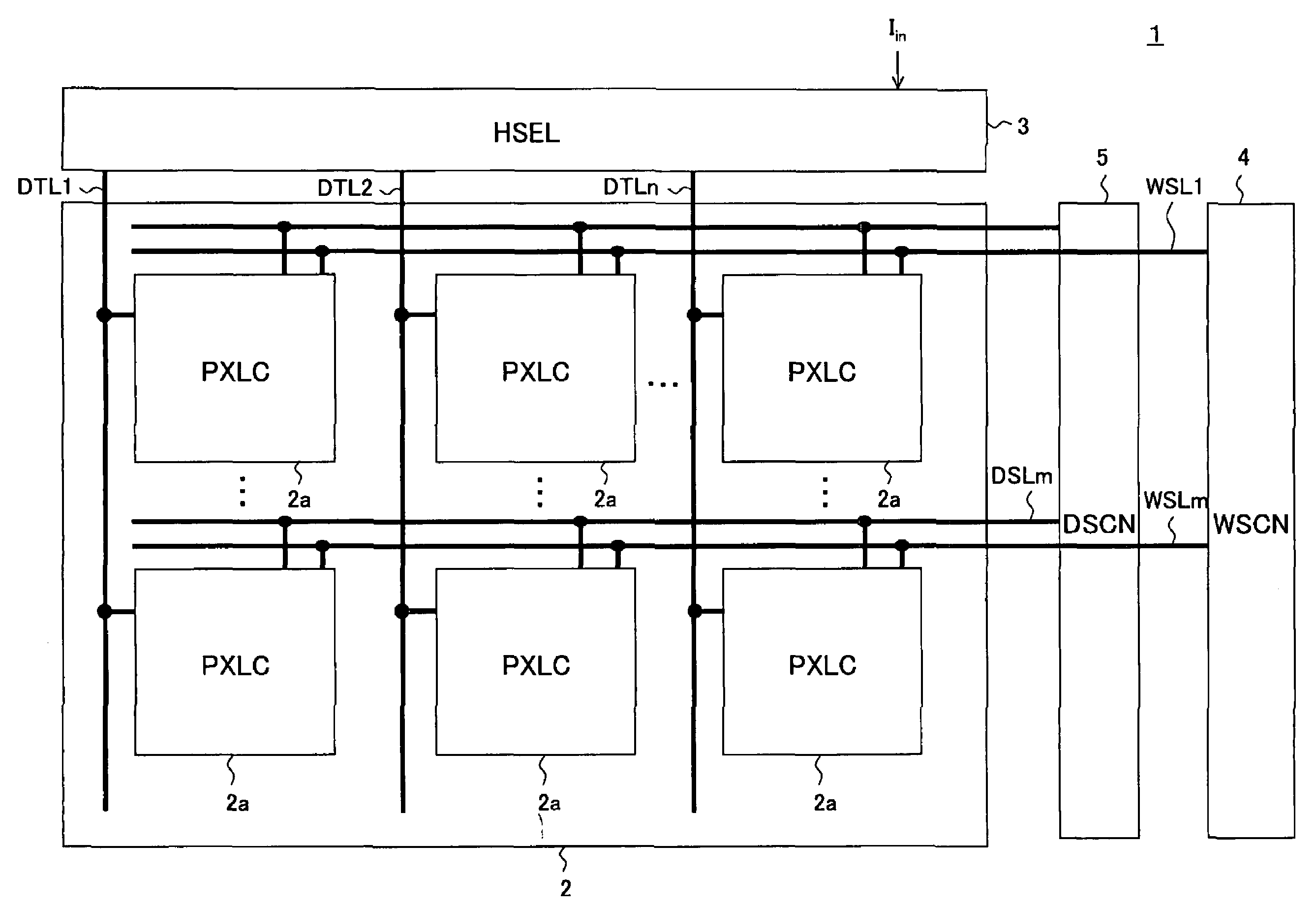
[0047]FIG. 8 is a block diagram of an example of the configuration of an organic EL display device employing a current drive system according to a first embodiment. FIG. 9 is a circuit diagram of the concrete configuration of a pixel circuit and a horizontal selector according to the first embodiment in the organic EL display device of FIG. 8.

[0048]This display device 100 has, as shown in FIG. 8 and FIG. 9, a pixel array 102 comprised of pixel circuits (PXLC) 101 arrayed in an m×n matrix, a horizontal selector (HSEL) 103, a write scanner (WSCN) 104, a drive scanner (DSCN) 105, data lines DTL101 to DTL10n selected by the horizontal selector 103 and sequentially supplied with the data signal in accordance with the luminance information as the current signal, scanning lines WSL101 to WSL10m selectively driven by the write scanner 104, and drive lines DSL101 to DSL10m selectively driven by the drive scanner 105.

[0049]Note that, in the pixel array 102, the pixel circuits 101 are arrayed ...

second embodiment

[0067]FIG. 12 is a block diagram of an example of the configuration of an organic EL display device employing the current drive system according to a second embodiment.

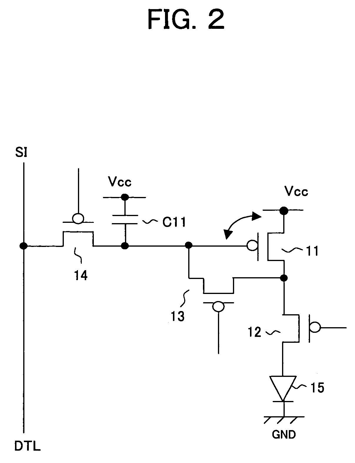
[0068]The difference of the second embodiment from the above first embodiment resides in that further a constant current source circuit comprised of n-channel TFTs 126 and 127 and a capacitor C122 is cascade connected (second stage serial connected) to the constant current source circuit comprising the TFTs 121 and 122 and the capacitor C121 between the node ND121 and the ground potential GND.

[0069]Here, this will be explained by taking a current sample and hold circuit 1031-1A as an example. The other current sample and hold circuits 1031-2A to 1031-nA have the same configuration as the current sample and hold circuit 1031-1A, so the explanation is omitted here.

[0070]In the current sample and hold circuit 1031-1A, the source of the second field effect transistor constituted by the TFT 121-1 is connected to the node N...


PUM


Abstract

A display device able to hold a drain potential of an output transistor functioning as a constant current source constant even in a sampling period of another circuit, able to suppress a change due to leakage of a gate potential of the output transistor, able to obtain a uniform current source free from variation in current value of an output stage, and able to display a high quality image without occurrence of uneven luminance toward a scanning end part, wherein for example a current sample and hold circuit finishing a sampling and holding operation during a period where the sampling and holding operation of its own stage is ended and another stage is performing a sampling and holding operation is configured so as to carry a constant current corresponding to a sampled current by a thin film transistor through a node by operating a leakage elimination circuit.

Description

BACKGROUND OF THE INVENTION[0001]1. Field of the Invention[0002]The present invention particularly relates to an organic electroluminescence (EL) display or other image display device comprising pixel circuits having electro-optical elements controlled in luminance by a current value arranged in a matrix, in particular a so-called active matrix type image display device wherein the value of the current flowing through an electro-optical element is controlled by an insulating gate type field effect transistor provided inside each pixel circuit.[0003]2. Description of the Related Art[0004]In an image display device, for example, a liquid crystal display, an image is displayed by arranging a large number of pixels in a matrix and controlling a light intensity for every pixel in accordance with image information to be displayed. The same is true for an organic EL display etc., but an organic EL display is a so-called self light emitting type display which has light emitting elements in ...

Claims


Application Information

Patent Timeline
Patent Type & Authority Patents(United States)
IPC IPC(8): G09G3/30G09G3/00G09G3/20H01L51/50G09G3/32G09G5/00H05B33/00H05B33/14
CPCG09G3/3233G09G3/3283G09G2300/0819G09G2320/043G09G2300/0861G09G2320/0223G09G2300/0842F15B21/001F15B11/028F15B21/14F15B2211/20515F15B21/042
Inventor YAMASHITA, JUNICHIUCHINO, KATSUHIDEYAMAMOTO, TETURO
Owner JOLED INC
Why Eureka
Try Eureka