Printed wiring board and method of manufacturing the same

a printing method and wiring board technology, applied in the direction of manufacturing tools, etching metal masks, printing element electric connection formation, etc., can solve the problems of difficult to form a good circuit, difficult to achieve good circuits, and inconvenient subtractive methods, so as to achieve high-density wiring designs, reduce the diameter of the land, and achieve easy high-density wiring designs.

Inactive Publication Date: 2007-07-17
CMK
View PDF16 Cites 4 Cited by
  • Summary
  • Abstract
  • Description
  • Claims
  • Application Information

AI Technical Summary

Benefits of technology

[0020]By thus eliminating a positional deviation between a blind via hole and a wiring pattern (concretely, a land formed around a blind via hole), it is possible to reduce the diameter of the land, with the result that high-density wiring design can be achieved.
[0035]Because a printed wiring board having a blind via hole is a constituent feature of the present invention, no positional deviation occurs between a blind via hole and a land. As a result, it is possible to reduce the diameter of the land, making it possible to easily achieve high-density wiring design.

Problems solved by technology

However, in the plating and an electrolytic plating to the whole insulating substrate when forming through-holes and blind-via-holes etc. and, therefore, the thickness of the conductor layer (metal foil plus a plating) to be etched becomes very large.
Therefore, it was difficult to form a good circuit.
Particularly, the subtractive method was not suitable for the formation of a fine wiring pattern having pattern line / pattern space of not more than 75 μm / 75 μm.
In contrast, the additive method, which is favorable for the formation of a fine wiring pattern, requires that a wiring pattern be formed by depositing a plating on an insulating layer and, therefore, compared to a case as in the subtractive method where an insulating substrate in which metal foil has been laminated on an insulating layer is processed, the additive method had problems such that the adhesion of the wiring pattern is poor.
Furthermore, in terms of the design of printed wiring patterns, wiring patterns are formed nonuniformly in the plane of the substrate and, therefore, when wiring patterns are formed by selective plating as in the additive method, currents are concentrated more than necessary in portions of coarse wiring patterns and variations in the thickness of the wiring pattern become large, resulting in problems such that it is difficult to ensure impedance matching.
Therefore, when all alignment accuracy is considered, the land diameter (equivalent to the above-described metal foil land 2a) becomes considerably large, thereby impairing high-density wiring design (this applies also to a manufacturing method which involves etching a window portion for laser beam machining in metal foil beforehand and then making a nonthrough hole).

Method used


Image

  • Printed wiring board and method of manufacturing the same
  • Printed wiring board and method of manufacturing the same
  • Printed wiring board and method of manufacturing the same

Examples


examples

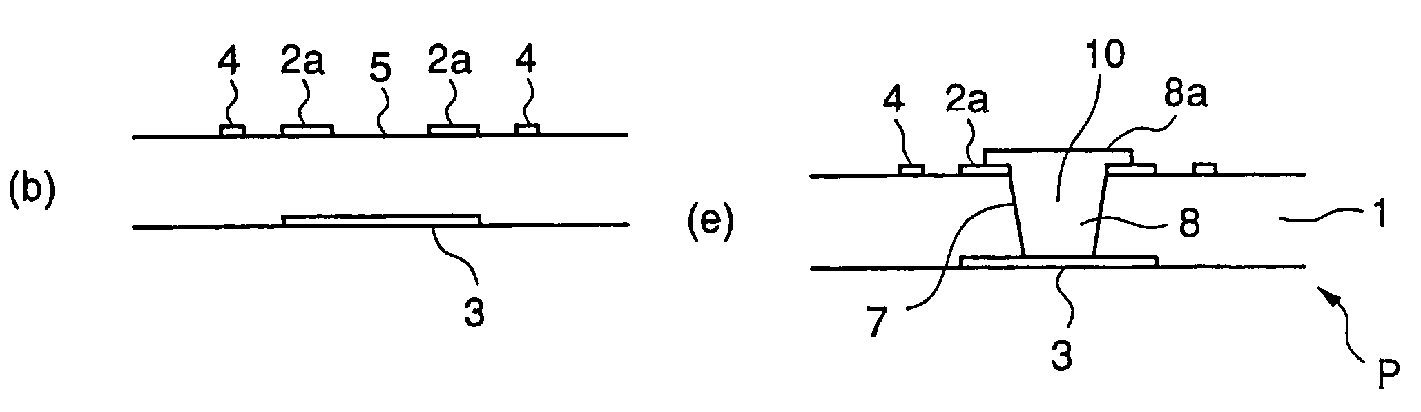
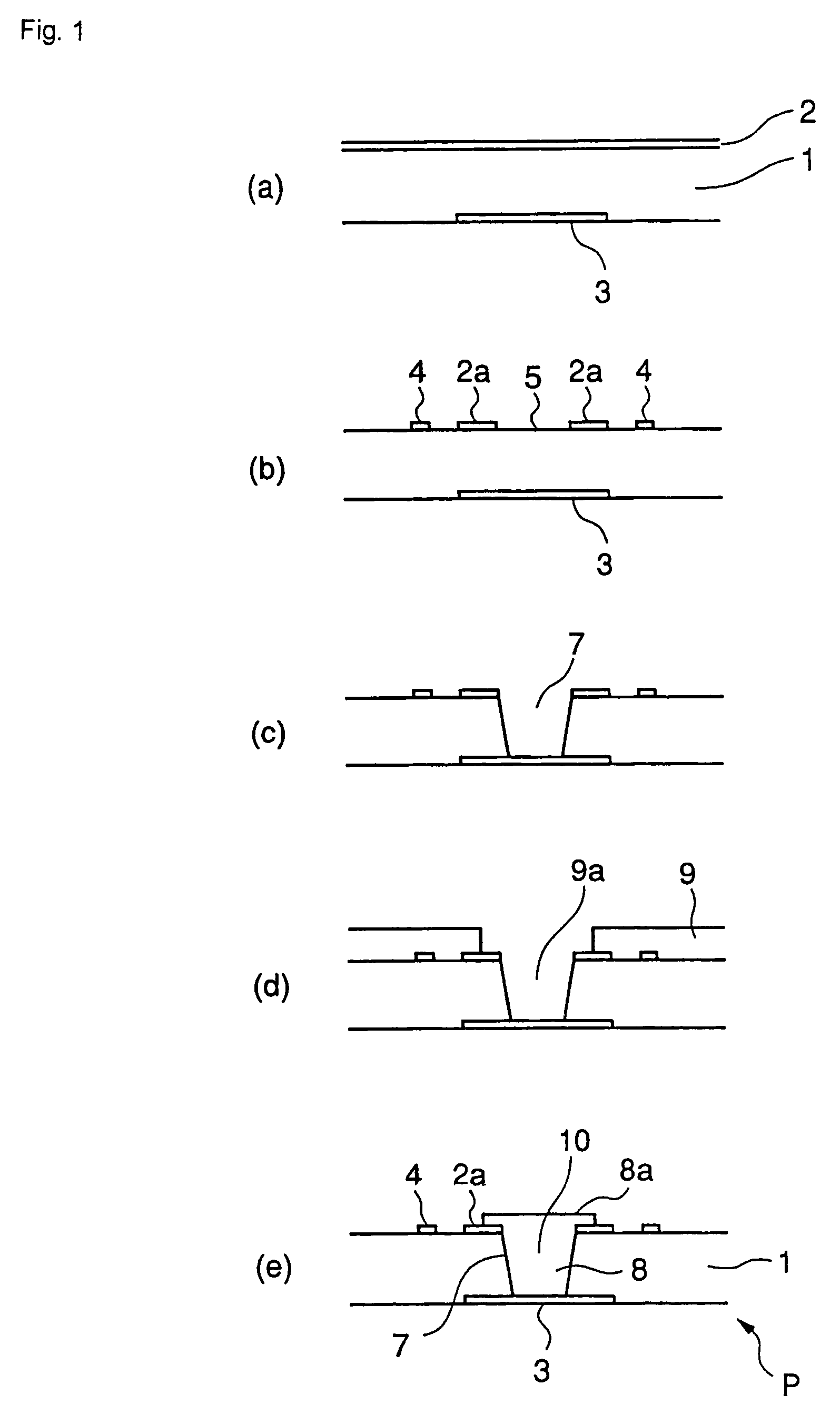
[0079]An embodiment of the present invention will be described with reference to FIGS. 5(l) to 5(h). Incidentally, a printed wiring board was fabricated in accordance with design specifications of line / space=30 μm / 30 μm.

[0080]Resin-including copper foil constituted by an insulating layer having a thickness of 60 μm and copper foil having a thickness of 12 μm was laminated on a core substrate on which a lower-layer wiring pattern is formed (equivalent to FIG. 5(a)) and a dry film for etching resist (made by Asahi Kasei Corporation: SPG 102) was laminated.

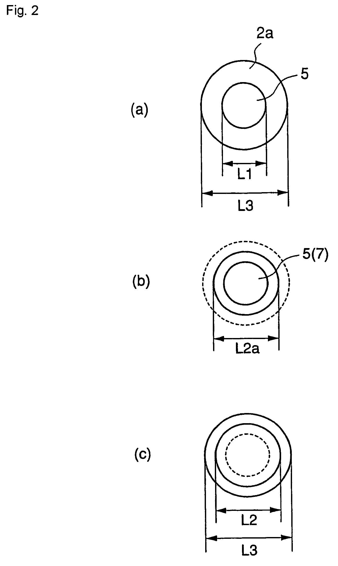
[0081]Next, by performing usual exposure and development (a 1% sodium carbonate aqueous solution) and etching (etchant: use of ferric chloride), an upper-layer wiring pattern (line 30 μm / space 30 μm), a metal foil (copper foil) land (φ150 μm) and a window portion (φ70 μm) were respectively formed (equivalent to FIG. 5(b))

[0082]Next, in order to suppress the deterioration of a bath of desmear treatment liquid during later desmear trea...


PUM

PropertyMeasurementUnit
sizeaaaaaaaaaa
diameteraaaaaaaaaa
diameteraaaaaaaaaa

Abstract

The present invention provides a printed wiring board in which there is no positional deviation between a blind via hole and a land and which enables high-density wiring design to be easily achieved. Provided is a method of manufacturing a printed wiring board in which wiring pattern forming layers are connected by a blind via hole, which includes the steps of forming a wiring pattern by etching at least metal foil laminated on a surface of an insulating layer and forming a land having a window portion in a portion where a blind via hole is to be formed; irradiating the window portion with a laser beam having a diameter larger than the diameter of the window portion but smaller than the diameter of the land, thereby making a nonthrough hole for forming the blind via hole; and forming a blind via hole by forming a plating on the nonthrough hole and the land.

Description

BACKGROUND OF THE INVENTION[0001]1. Field of the Invention[0002]The present invention relates to a printed wiring board and a method of manufacturing the printed wiring board and, more particularly, to a printed wiring board having a fine wiring pattern of high-density wiring design and a method of manufacturing the printed wiring board.[0003]2. Description of the Related Art[0004]Methods of forming a circuit in a printed wiring board are divided into the subtractive method which involves forming an etching resist pattern on metal foil, such as copper foil, and forming a wiring pattern by etching the part of metal foil not covered by the etching resist pattern; and the additive method which involves forming a plating resist of a pattern reverse to a circuit and forming a wiring circuit by depositing a plating on an opening of this plating resist.[0005]Because the manufacturing steps in the subtractive method are easier than in the additive method, it is possible to manufacture circu...

Claims


Application Information

Patent Timeline
Patent Type & Authority Patents(United States)
IPC IPC(8): H01K3/10
CPCH05K3/0008H05K3/0035H05K3/421H05K3/428H05K2201/0969Y10T29/49126Y10T29/49117Y10T29/49155Y10T29/49144Y10T29/49165H05K2203/0554H05K1/11H05K3/42
Inventor HIRATA, EIJI
Owner CMK
Why Eureka
Try Eureka