
Electrophotographic photosensitive member

a photosensitive member and electrophotography technology, applied in the field of electrophotography photosensitive members, can solve the problems of difficult absorption of surface layers, difficult to achieve image deletion phenomena, and difficult to achieve phenomenon such as the above-described image deletion phenomenon, and achieve good electrophotographic properties. , the effect of minimizing light absorption

Inactive Publication Date: 2007-08-14
CANON KK
View PDF10 Cites 23 Cited by
  • Summary
  • Abstract
  • Description
  • Claims
  • Application Information

AI Technical Summary

Benefits of technology

The solution enables the production of electrophotographic photosensitive members with reduced light absorption at short wavelengths, improved chargeability, and enhanced resolution, allowing for high-quality, high-speed image output with reduced defects and increased durability.

Problems solved by technology

In addition, an a-Si photosensitive member has a surface layer having a hardness much higher than that of an organic photosensitive member or the like, so the surface layer is difficult to abrade and a corona product is apt to remain on the surface.
As a result, an image deletion phenomenon may occur.
Therefore, it is difficult for a phenomenon such as the above-described image deletion to occur.
In addition, toner having a small particle size to be used for a high-resolution digital full-color copying machine tends to present problems such as a transfer residue on the surface of a photosensitive member and a cleaning residue.
However, the surface layer is gradually abraded inevitably owing to rubbing in a copying machine, so the layer must secure at least a certain thickness.
Accordingly, an increase in absorbed amount due to an increase in thickness and sensitivity unevenness due to abrasion unevenness may present a problem in some cases when high-resolution images are to be stably outputted.
In this case, however, the film has a structure close to that of a polymer, and its hardness may be low or its resistance value may be too high.
However, a film made of such material can be hardly used for the surface layer of a photosensitive member, and it has not been put into practical use yet.
Therefore, light is expected to be absorbed to some extent at a wavelength of, for example, around 400 nm, ans a sufficient sensitivity may not be obtained.

Method used


Image

  • Electrophotographic photosensitive member
  • Electrophotographic photosensitive member
  • Electrophotographic photosensitive member

Examples


example 1

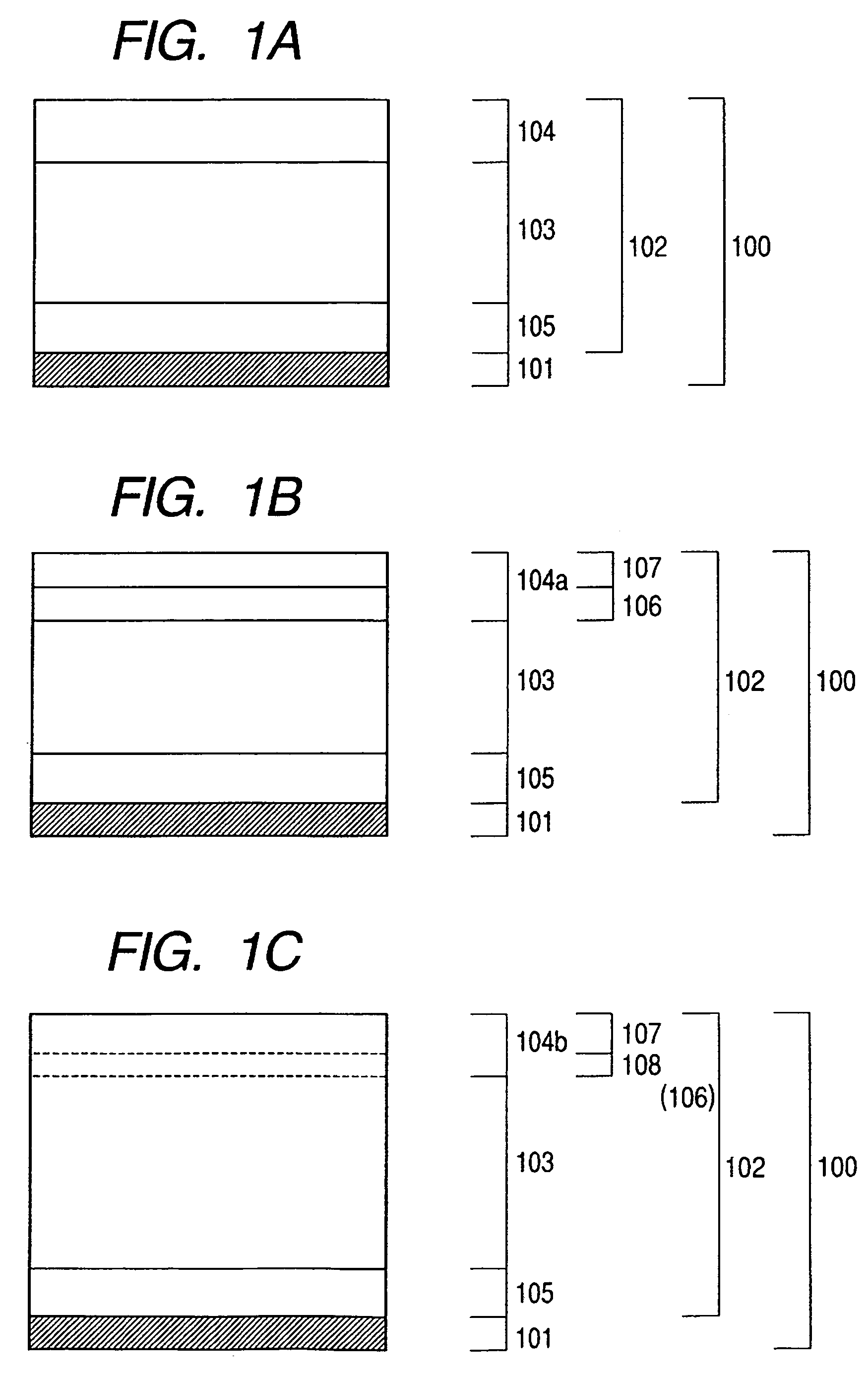
[0282]A plasma CVD apparatus shown in FIG. 2 was used to sequentially superimpose deposition films under the conditions shown in Table 1 on an aluminum cylinder (support), which had a diameter of 84 mm and a length of 381 mm and was subjected to mirror finish, to thereby produce a photosensitive member composed of a top injection-blocking layer and a surface layer. All lower injection-blocking layers and photoconductive layers were produced under the conditions shown in Table 1 as common conditions. Surface layers were produced under the conditions shown in Table 2 for the flow rate of an SiH4 gas, the mixing ratio between SiH4 and N2 and electric energy per amount of an SiH4 gas, and under the conditions shown in Table 1 for the others. Thus, photosensitive members A to H different from each other in nitrogen atom concentration in a surface layer were produced.

[0283]The photosensitive members A to H thus produced were evaluated as follows.

[0284]Each photosensitive member was set in...

example 2

[0296]A plasma CVD apparatus shown in FIG. 2 was used to sequentially superimpose deposition films composed of a lower injection-blocking layer, a photoconductive layer, a top injection-blocking layer, and a surface layer under the conditions shown in Table 3 on an aluminum cylinder (support), which had a diameter of 84 mm and a length of 381 mm and was subjected to mirror finish, to thereby produce a photosensitive member. All lower injection-blocking layers and photoconductive layers were produced under the conditions shown in Table 1 as common conditions. Surface layers were produced with the flow rate of a CH4 gas changed variously as shown in Table 4. Thus, photosensitive members 2A to 2H different from each other in carbon atom concentration in a surface layer were produced.

[0297]Each of the photosensitive members 2A to 2H thus produced was evaluated for the following items in addition to (1) a nitrogen atom concentration and (3) the property of transmitting light having a wav...

example 3

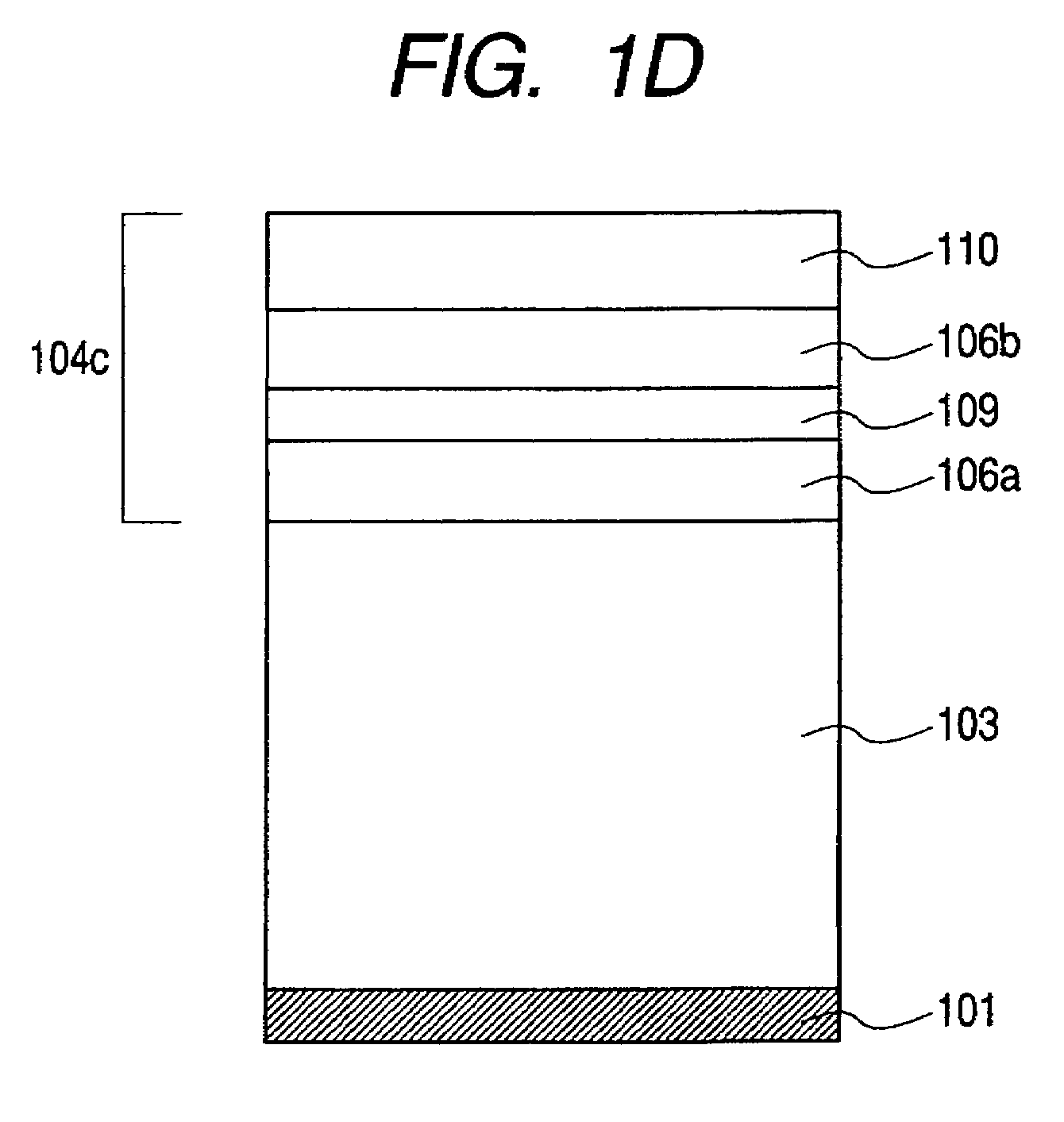
[0305]A plasma CVD apparatus shown in FIG. 2 was used to sequentially superimpose deposition films composed of a lower injection-blocking layer, a photoconductive layer, and a surface region layer under the conditions shown in Table 5 on an aluminum cylinder (support), which had a diameter of 84 mm and a length of 381 mm and was subjected to mirror finish, to thereby produce a photosensitive member.

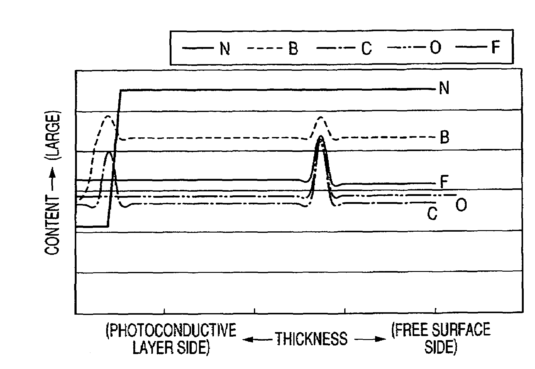
[0306]In this case, each of a carbon atom concentration and a boron atom concentration (boron is a Group 13 element in the periodic table) was caused to have a local maximum value by changing the amount of each of a CH4 gas and a B2H6 gas to be introduced during the formation of a surface region layer. A method of introducing a gas for forming a local maximum value in a surface region layer shown in Table 3 involved: increasing the amount of each of the CH4 gas and the B2H6 gas from a certain value in a linear fashion over a predetermined time period as shown in Table 5 when forming the c...


PUM


Abstract

An electrophotographic photosensitive member is provided minimizing the absorption of image exposure having a short wavelength in a surface layer and keeping good electrophotographic properties including resolving power. The electrophotographic photosensitive member includes a conductive substrate, and a photoconductive layer and a surface region layer sequentially superimposed on the conductive substrate. The surface region layer is composed of a non-single-crystal silicon nitride film containing an Group element in the periodic table and a carbon atom and using at least a silicon atom and a nitrogen atom as base materials. In the surface region layer, the Group 13 element content with respect to the total amount of constituent atoms has distribution having at least two local maximum values in the thickness direction, and an the average concentration of nitrogen atoms is 30 atm % to 70 atm %.

Description

[0001]This application is a continuation of International Application No. PCT / JP2005 / 023188, filed Dec. 12, 2005, which claims the benefit of Japanese Patent Application No. 2004-358096, filed Dec. 10, 2004 and Japanese Patent Application No. 2004-358098, filed Dec. 10, 2004.BACKGROUND OF THE INVENTION[0002]1. Field of the Invention[0003]The present invention relates to an electrophotographic photosensitive member. In particular, the present invention relates to an electrophotographic photosensitive member optimum for a printer, a facsimile, a copying machine, or the like using light having a relatively short wavelength of 380 nm or more and 500 nm or less for exposure.[0004]2. Related Background Art[0005]In the field of image formation, a photoconductive material in a photosensitive member is requested to have properties including the following properties:1. High sensitivity and a high SN ratio (photo current (Ip) / dark current (Id))2. An absorption spectrum suited for the spectral ...

Claims


Application Information

Patent Timeline
Patent Type & Authority Patents(United States)
IPC IPC(8): G03G5/14
CPCG03G5/08228G03G5/08242G03G5/08257G03G5/08285G03G5/14704
Inventor KOJIMA, SATOSHIAOKI, MAKOTOOHIRA, JUNOWAKI, HIRONORIHOSOI, KAZUTOYAMADA, MOTOYA
Owner CANON KK
Learn More