Semiconductor laser device

a laser device and semiconductor technology, applied in the direction of lasers, semiconductor laser structural details, semiconductor lasers, etc., can solve the problems of limited field in which this device can be applied, and the characteristics of the semiconductor laser cannot be satisfied, so as to reduce shorten the time needed for laser drive initiation. , the effect of reducing the time needed for warm-up

Active Publication Date: 2007-08-14
NICHIA CORP
View PDF8 Cites 11 Cited by
  • Summary
  • Abstract
  • Description
  • Claims
  • Application Information

AI Technical Summary

Benefits of technology

[0017]According to the semiconductor laser device of the present invention, the impedance during laser drive initiation can be stabilized. This allows the time needed for warm-up to be shortened, the oscillations of the laser light to occur more quickly, the loss of time to be eliminated, and a fast response time to be achieved in devices which employ a semiconductor laser. Moreover, because oscillations will quicken, the threshold value will be reduced, oscillation at a low current will be made possible, and low energy consumption can be achieved. Furthermore, the impedance during laser drive initiation can be stabilized, noise can be reduced, and a high performance and high quality semiconductor laser device can be achieved.

Problems solved by technology

Even if the serial resistance of the conventional semiconductor laser is reduced as described above, this semiconductor laser cannot achieve satisfactory characteristics depending on the type of semiconductor layer that has the active layer, and there are limits on the fields in which this device can be applied.

Method used


Image

  • Semiconductor laser device
  • Semiconductor laser device
  • Semiconductor laser device

Examples


embodiment 1

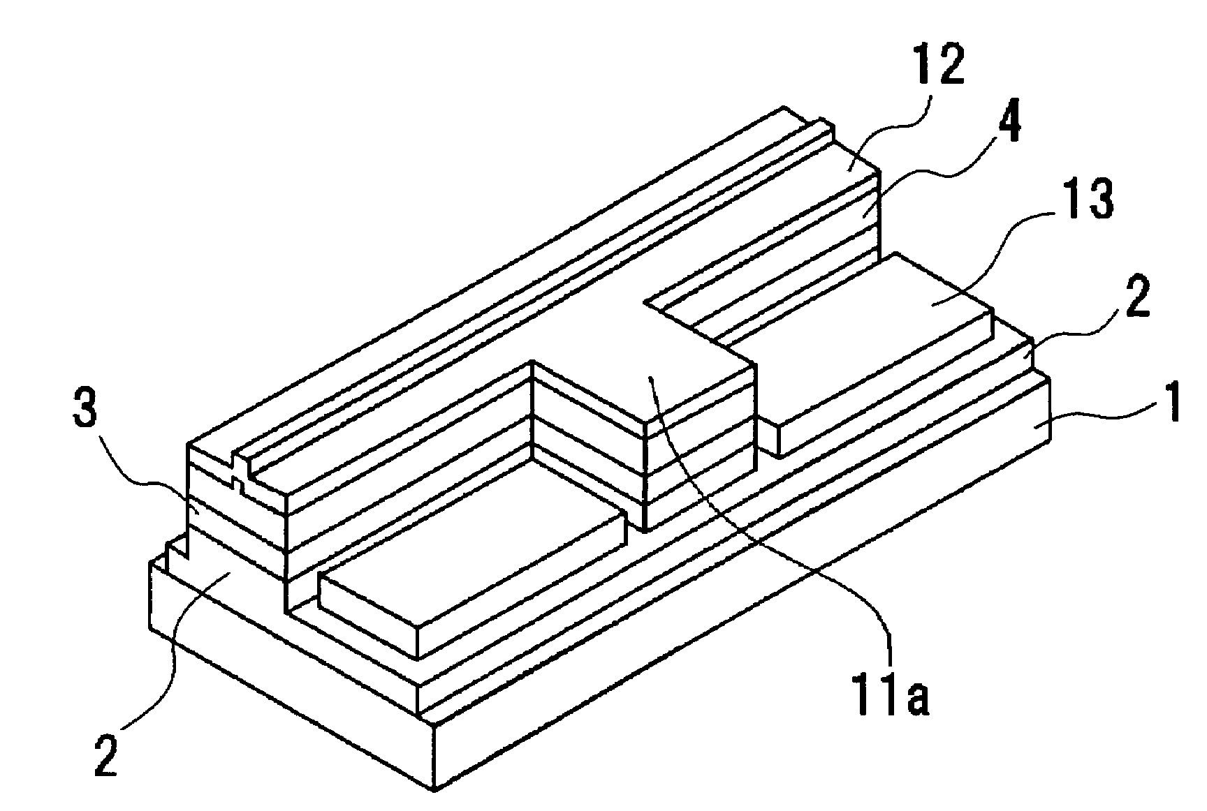
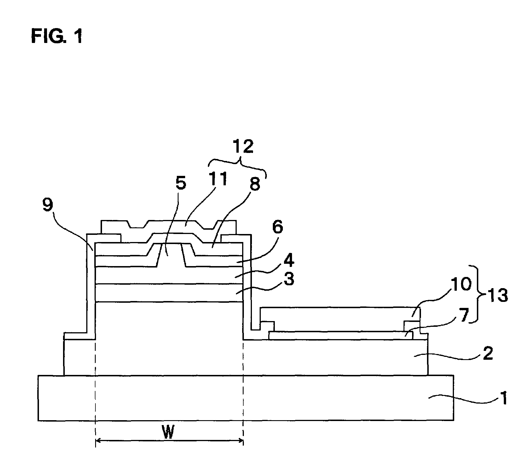
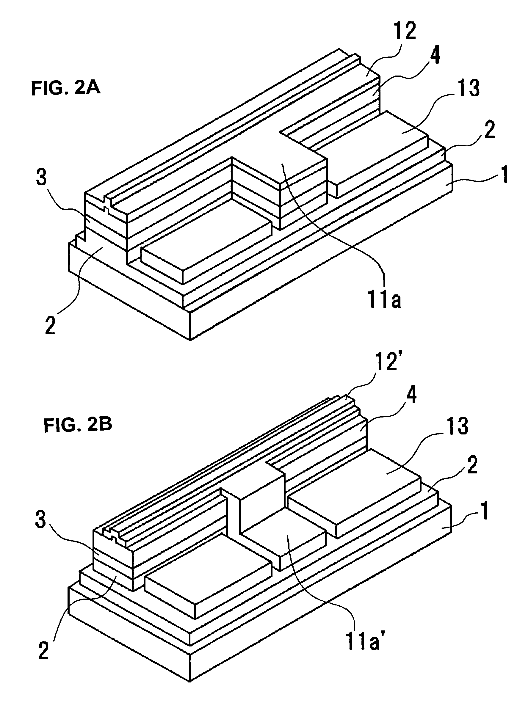
[0059]As shown in FIGS. 1 and 2A, the semiconductor laser device of this embodiment is formed by sequentially laminating an n-type semiconductor layer 2 that is the first conductive type semiconductor layer, an active layer 3, and a p-type semiconductor layer 4 that is the second conductive type semiconductor layer on a substrate 1.

[0060]A portion of the n-type semiconductor layer 2 is removed in the film thickness direction, as well as portions of the active layer 3 and the p-type semiconductor layer 4 disposed thereon. In addition, a stripe shaped ridge 5 is formed on the upper surface of the p-type semiconductor layer 4.

[0061]A first insulating film 6 is formed on the upper surface of the p-type semiconductor layer 4, and covers the lateral surfaces of the ridge 5 but not the upper surface thereof. In addition, an n-type ohmic electrode 7 that is partially connected with the n-type semiconductor layer 2 is formed on the upper surface of the n-type semiconductor layer 2 from which...

embodiment 2

[0093]As shown in FIG. 2B, the semiconductor laser device of this embodiment is substantially the same as the semiconductor laser device of FIGS. 1 and 2A, except that a portion of the n-type semiconductor layer 2 in the depth direction, the active layer 3, and the p-type semiconductor layer 4 are formed into a stripe shape, a second electrode 12′ is formed on this laminated structure, and a projection 11a′ of a pad electrode that forms the second electrode 12′ is disposed across the top of the n-type semiconductor layer 2 via an insulating layer (not shown in the figure).

[0094]The semiconductor laser device described above can be formed by substantially the same method as described above. Note that after the pad electrode is formed, the semiconductor layers are etched by RIE until the sapphire substrate is exposed in a mesh pattern in order to make the semiconductor layers chip sized. At this point, the laser discharge surface will be etched directly in front of the laser discharge...


PUM


Abstract

A laser device is disclosed which stabilizes impedance at laser drive initiation, and in which an oscillation at low current, a high reaction speed, a low noise, and the like are achieved. A semiconductor laser device includes first and second conductive type semiconductor layers, an active layer, and first and second electrodes. The second electrode comprises an ohmic electrode and a pad electrode. The first electrode is formed on the same planar side of the first conductive type semiconductor layer as the second electrode, and is disposed in the same direction as the pad electrode with respect to the ohmically connected region. The second conductive type semiconductor layer is set to a width that can secure light confinement on both sides of the ohmically connected region.

Description

BACKGROUND OF THE INVENTION[0001]1. Field of the Invention[0002]The present invention relates to a semiconductor laser device, and more particularly to a semiconductor laser device that employs a Group III-V nitride semiconductor.[0003]2. Discussion of the Related Art[0004]In recent years, semiconductor lasers have been changing to smaller, more lightweight, more highly reliable, and higher output lasers, and they have been used as a light source for electronic devices such as DVD players, medical devices, and other similar devices. For these semiconductor devices, Group III-V nitride semiconductors are studied because they are capable of generating light at relatively short wavelengths.[0005]For example, as shown in FIG. 6, a semiconductor laser includes nitride semiconductors comprising a GaN layer 21, an n-type GaN layer 22, an n-type AlGaN cladding layer 23, an n-type GaN light confinement layer 24, an active layer 25 (e.g., an InGaN multiple quantum well layer), a p-type GaN li...

Claims


Application Information

Patent Timeline
Patent Type & Authority Patents(United States)
IPC IPC(8): H01S5/00H01S5/02H01S5/042H01S5/062H01S5/22H01S5/223H01S5/323H01S5/343
CPCB82Y20/00H01S5/0425H01S5/2231H01S5/32341H01S5/34333H01S5/0213H01S5/0422H01S5/06226H01S5/2214H01S2301/173H01S2304/04H01S5/04257H01S5/04256
Inventor YONEDA, AKINORI
Owner NICHIA CORP
Why Eureka
Try Eureka