
Cell library database and timing verification and withstand voltage verification systems for integrated circuit using the same

a technology of voltage verification and integrated circuit, applied in the field of cell library databases, can solve the problems of preventing a total logical verification including a power control, affecting the accuracy of timing verification, and increasing leakage current during standby, and achieve good timing verification

Inactive Publication Date: 2007-08-14
SOCIONEXT INC
View PDF9 Cites 3 Cited by
  • Summary
  • Abstract
  • Description
  • Claims
  • Application Information

AI Technical Summary

Benefits of technology

[0007]The object of the present invention is to provide a cell library database structure which is capable of flexibly handling not only power on / off techniques but also future environments for designing a semiconductor integrated circuit, including variable power supply techniques, and which is capable of conducting, even on a semiconductor integrated circuit to which those techniques are applied, good logical and timing verifications and in addition withstand voltage verification of each element therein.
[0021]In the present invention, in addition, an analog input terminal or an analog output terminal is provided with voltage value information in which different voltage states of one node are represented in multiple bits, thereby enabling a total logical verification to which is also subjected an analog interface on circuitry embedded with analog and digital subcircuits.
[0022]Furthermore, in the present invention, the cell library database contains information on logic delays between the input and output signals when logic changes occur therebetween, thereby enabling timing verification.
[0023]Moreover, in the present invention, the cell library database contains withstand voltage information, thereby enabling withstand voltage verification.
[0024]In the timing verification system for an integrated circuit of the present invention, the basic circuits each have logic delay information for each piece of voltage information of the power source. This enables even semiconductor circuit design using a variable power supply technique to conduct a good timing verification when a dynamic change of source voltage is repeated during operation.
[0025]The withstand voltage verification system for an integrated circuit of the present invention can compare voltage value information given to the data terminals with withstand voltage information. This makes it possible to conduct withstand voltage verification on input signals to data terminals, one or more output signals from one or more data terminals and source voltages given to a data terminal.

Problems solved by technology

In recent years, a decrease in the threshold voltage of a transistor of a semiconductor integrated circuit accompanied with miniaturization of the circuit, however, has caused a big problem of an increase in leakage current during standby.
In conducting logical verification on a semiconductor integrated circuit employing this technique in which the power supply is started and stopped, employment of the library database structure in FIG. 7 causes the following problems.
This prevents a total logical verification including a power control thereof.
Second, though the logic delay time between input and output signals at start up of the power source is different from the delay time between input and output signals under normal operation, the database only contains delay time information in the condition in which a steady power is supplied.
This prevents an accurate timing verification in consideration of the delay time between the input and output signals at the start up of the power source.

Method used


Image

  • Cell library database and timing verification and withstand voltage verification systems for integrated circuit using the same
  • Cell library database and timing verification and withstand voltage verification systems for integrated circuit using the same
  • Cell library database and timing verification and withstand voltage verification systems for integrated circuit using the same

Examples


first embodiment

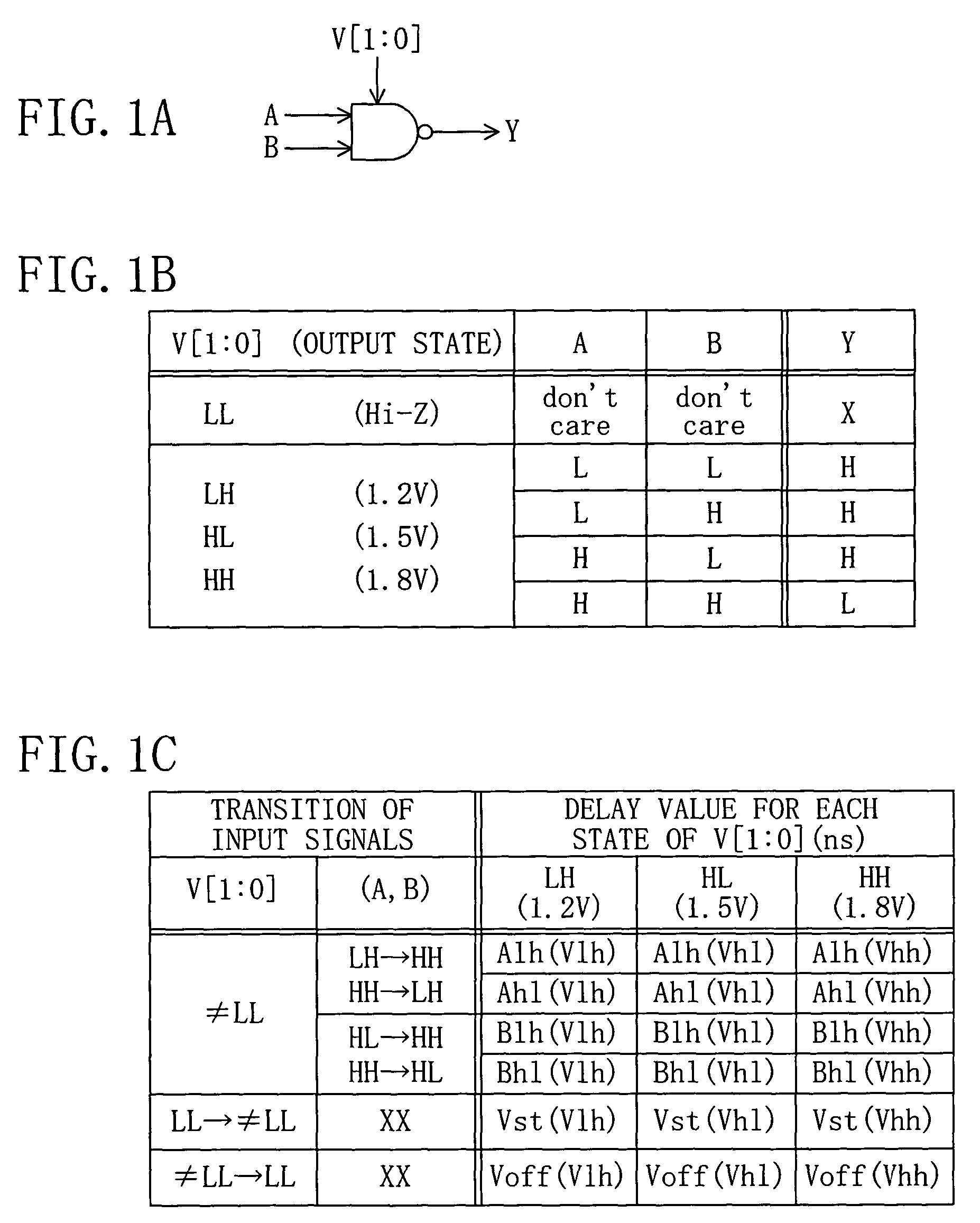
[0036]FIG. 1 shows a cell library database of a first embodiment of the present invention.

[0037]In FIG. 1, FIG. 1A illustrates a symbol for a cell library of a NAND gate as an exemplary basic circuit. The symbol includes four data terminals A, B, Y and V, of which the data terminals A and B are digital signal input terminals, the data terminal Y is a digital signal output terminal, and the data terminal V is a power source terminal for receiving a source voltage. In the following discussion, input signals to the input terminals A and B, source voltage signals to the power source terminal V, and output signals from the output terminal Y are also marked with the same letters as those indicating the respective terminals. FIG. 1B shows a truth table for logics relative to input signals A and B and a source voltage signal V illustrated in FIG. 1A. FIG. 1C lists various pieces of information on logic delays of the NAND gate occurring between the time the input signals A, B and V are each ...

second embodiment

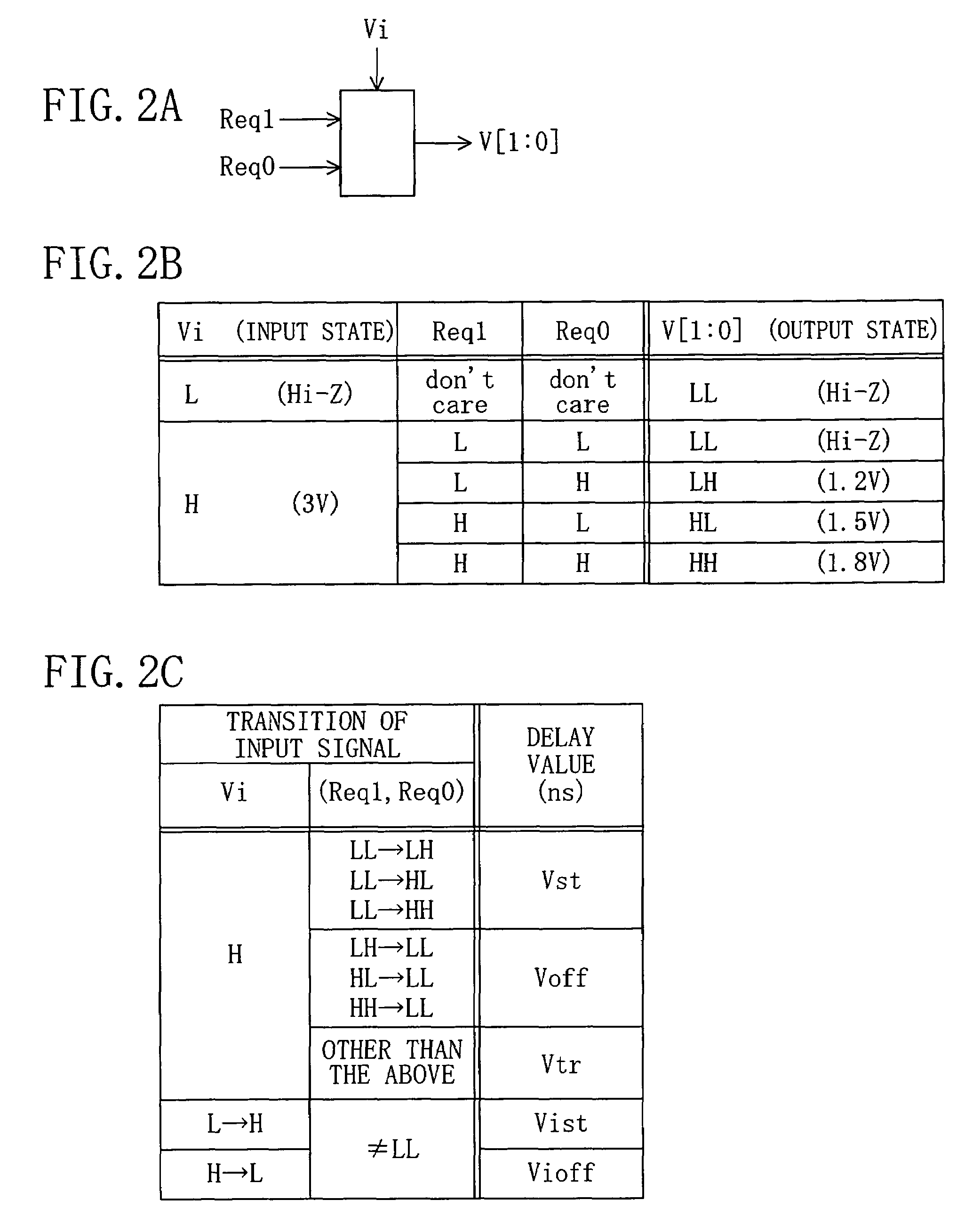
[0043]Next discussion will be made of a cell library database of a second embodiment of the present invention. The second embodiment exemplarily employs a voltage conversion cell as a basic circuit.

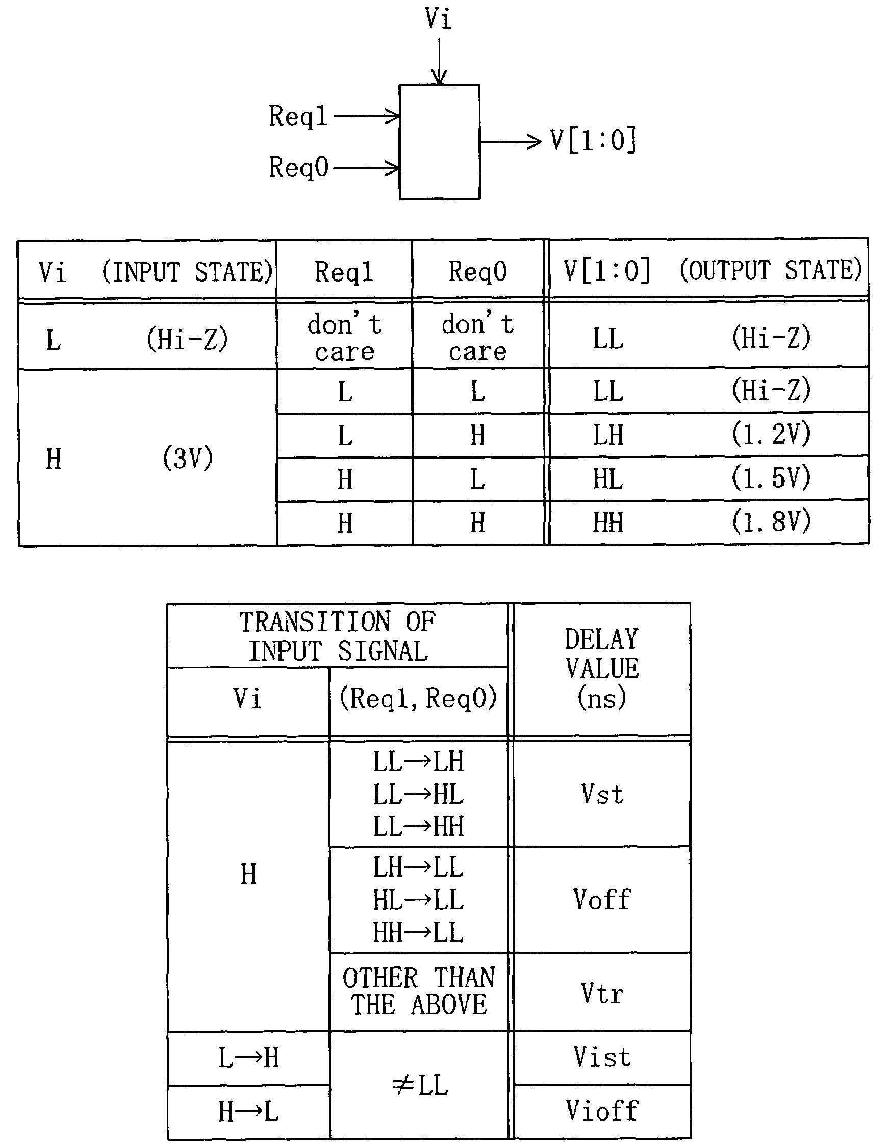
[0044]In FIG. 2, FIG. 2A shows a symbol for the voltage conversion cell, which includes four data terminals Req1, Req0, Vi and V. The data terminals Req1 and Req0 are signal input terminals, the data terminal Vi is a power source terminal for receiving a source voltage, and the data terminal V is a voltage output terminal. FIG. 2B shows a truth table of output voltage values V [1:0] relative to the input signals Req1 and Req0 and the source voltage signal Vi illustrated in FIG. 2A. FIG. 2C lists information on logic delays between the input and output terminals of the voltage conversion cell when logic changes occur therebetween, that is, various pieces of information on logic delays occurring between the time the input signals Req1, Req0 and Vi are each changed and the time the output si...

third embodiment

[0054]FIG. 3 shows a timing verification system for an integrated circuit according to a third embodiment of the present invention.

[0055]The third embodiment employs the cell library database of the NAND cell shown in FIG. 1 and the cell library database of the voltage conversion cell shown in FIG. 2 to conduct timing verification on LSIs in a variable power supply system capable of varying the source voltage arbitrarily.

[0056]FIG. 3 shows an integrated circuit using two NAND gates 1 illustrated in FIG. 1 and a voltage conversion cell 2 illustrated in FIG. 2. This circuit in FIG. 3 is configured to obtain an output signal Y based on pieces of logical information of three input signals A, B and C, in which the output voltage V [1:0] from the voltage conversion cell 2 is supplied to the two NAND gates 1 as a source voltage.

[0057]As can be seen from the cell library database of the NAND cell shown in FIG. 1, in the third embodiment, each NAND cell 1 can obtain source voltage value info...


PUM


Abstract

In a cell library database, timing verification is conducted on an LSI which exists in a variable power supply system capable of changing the source voltage arbitrarily and which includes logic delay information associated with a plurality of source voltages. The database is configured, for example, so that the voltage information V of the source is represented in multiple bits V [1:0] and delay times Alh (Vlh) to Bhl (Vhh) between the time input signals A and B are each changed and the time the output signal Y changes are described for respective pieces of source voltage information LH (1.2 V), HL (1.5 V) and HH (1.8 V). This allows timing verification in the variable source system which operates with the source voltage changed dynamically.

Description

BACKGROUND OF THE INVENTION[0001]The present invention relates to cell library databases used in computer-aided design (CAD) for logic circuits such as semiconductor integrated circuits and design aiding systems employing this database. Particularly, the present invention relates to cell library databases and timing verification and withstand voltage verification systems of integrated circuits which are appropriate for logical verification, timing verification of delay or the like, failure analysis, and logical verification used in a software development tool.[0002]Generally, computer-aided design (CAD) for a logic circuit such as a semiconductor integrated circuit has conventionally adopted, as a cell library database used for the CAD, a database structure which includes a symbol as shown in FIG. 7A, logical information as shown in FIG. 7B, and logic delay information as shown in FIG. 7C. The symbol shown in FIG. 7A is a logic component indicating a logical product (referred herein...

Claims


Application Information

Patent Timeline
Patent Type & Authority Patents(United States)
IPC IPC(8): G06F17/50
CPCG06F17/5022G06F30/33
Inventor SAKIYAMA, SHIROMOCHIZUKI, KOUJI
Owner SOCIONEXT INC
Learn More