

Data latch circuit of semiconductor device
a technology of data latching and semiconductor devices, applied in digital storage, pulse automatic control, instruments, etc., can solve the problems of failure condition, increased charge/discharge current consumption, and above-mentioned problem becoming more serious, so as to prevent unnecessary charge/discharge current consumption and latching stably
- Summary
- Abstract
- Description
- Claims
- Application Information
AI Technical Summary
Benefits of technology
Problems solved by technology
Method used
Image

Examples
Embodiment Construction
[0040]Hereinafter, a data latch circuit in accordance with the present invention will be described in detail referring to the accompanying drawings.
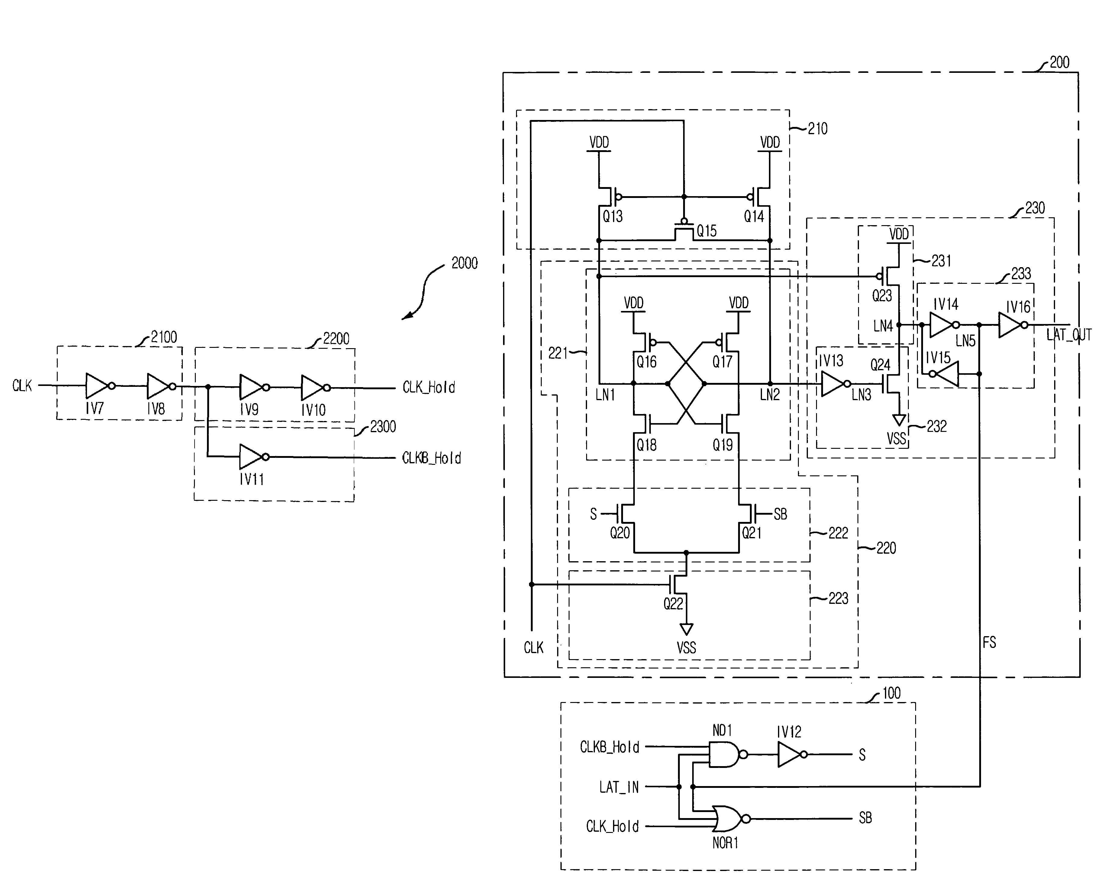
[0041]FIG. 4 is a data latch circuit in accordance with a preferred embodiment of the present invention.
[0042]As shown, the data latch circuit includes a hold time delay unit 2000, a data input control unit 100 and a data latch unit 200.
[0043]The hold time delay unit 2000 delays a clock signal CLK for a hold time of a data signal to thereby generate a first clock signal CLK_Hold. The hold time delay unit 2000 also generates a second clock signal CLKB_Hold which is an inverted version of the first clock signal CLK_Hold.
[0044]The data input control unit 100 generates a first data transition detection signal S in response to a first transition timing of the first clock signal CLK_Hold and a data signal LAT_IN0 and generates a second data transition detection signal SB in response to a second transition timing of the second clock signal CLKB...
PUM
 Abstract
Description
Claims
Application Information