Anisotropic conductive sheet, production process, contact structure, electronic device and inspection apparatus for operation test

a technology of anisotropic conductive sheet and contact structure, which is applied in the direction of connection contact material, coupling device connection, instruments, etc., can solve the problems of difficult realization of contactor capable of simultaneously coming into contact, the inability of general purpose use of handling devices, and the inability to realize contactors, etc., to achieve simple production process, low production cost, and long life span

Inactive Publication Date: 2007-09-11
FUJITSU LTD
View PDF22 Cites 27 Cited by
  • Summary
  • Abstract
  • Description
  • Claims
  • Application Information

AI Technical Summary

Benefits of technology

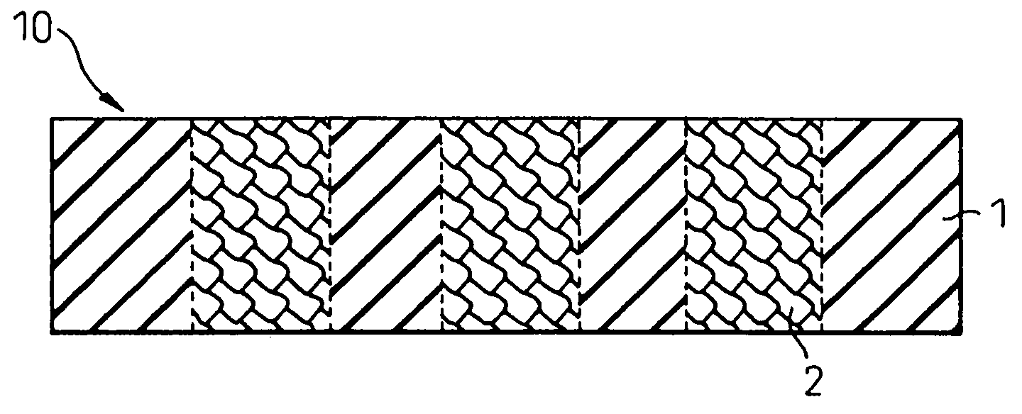
[0027]An object of the present invention is to solve the above problems, thereby providing an anisotropic conductive sheet characterized in that: the life span is long; it is possible to cope with a small pitch; a predetermined electrical connection can be attained; the circuit devices are not polluted; the production process is simple; and the production cost is low.
[0028]Another object of the present invention is to provide an anisotropic conductive sheet showing no bleeding out of silicone oil.

Problems solved by technology

When chip sizes are different from each other, the handling device cannot be used for general purpose.
Therefore, it is very difficult to realize a contactor capable of simultaneously coming into contact with a plurality of terminals of LSI which is kept in the state of a wafer and, if possible, a contactor capable of simultaneously coming into contact with all terminals of LSI on a wafer all at once.
Realization of such a contactor has become a common problem to be solved in the industry.
However, the above probes are disadvantageous as follows.
The costs of both the needle type mechanical probe and membrane type probe are high.
Further, in the former needle type mechanical probe, as the individual pins are obliquely arranged, the arrangement and positional accuracy of needle ends are limited.
However, these and other anisotropic conductive elastomer sheets of the prior art still leave room for improvements.
(a) The life span is short.
Therefore, the above problems become remarkable.
(b) It is impossible to cope with a small pitch.
It is difficult to incorporate conductive material into the anisotropic conductive sheet.
(c) It is impossible to accomplish a predetermined electrical connection.
As the mechanical strength of this oxide film of aluminum is high, when the sheet is connected with an electrode, it is difficult for the electrical conductive passage section of the sheet to pierce the oxide film of aluminum.
As a result, it is impossible to attain a predetermined electrical connection.
Especially when the sheet is connected with the electrodes all at once, although the sheet can be partially connected with the electrodes, it is impossible to connect the sheet with all the electrodes uniformly and stably.
(d) Circuit apparatus and others are polluted.
However, since this silicone rubber contains silicone oil of low molecular weight, for example, when the elastomer sheet is used for the inspection of a circuit device over a long period of time, silicone oil bleeds out onto the sheet surface.
By this silicone oil bleeding out onto the sheet surface, a surface of the electrode to be inspected, which is an object of inspection, is polluted.
As a result, when the circuit device is mounted, it becomes impossible to conduct bonding and further it becomes impossible to attain a predetermined electrical connection.
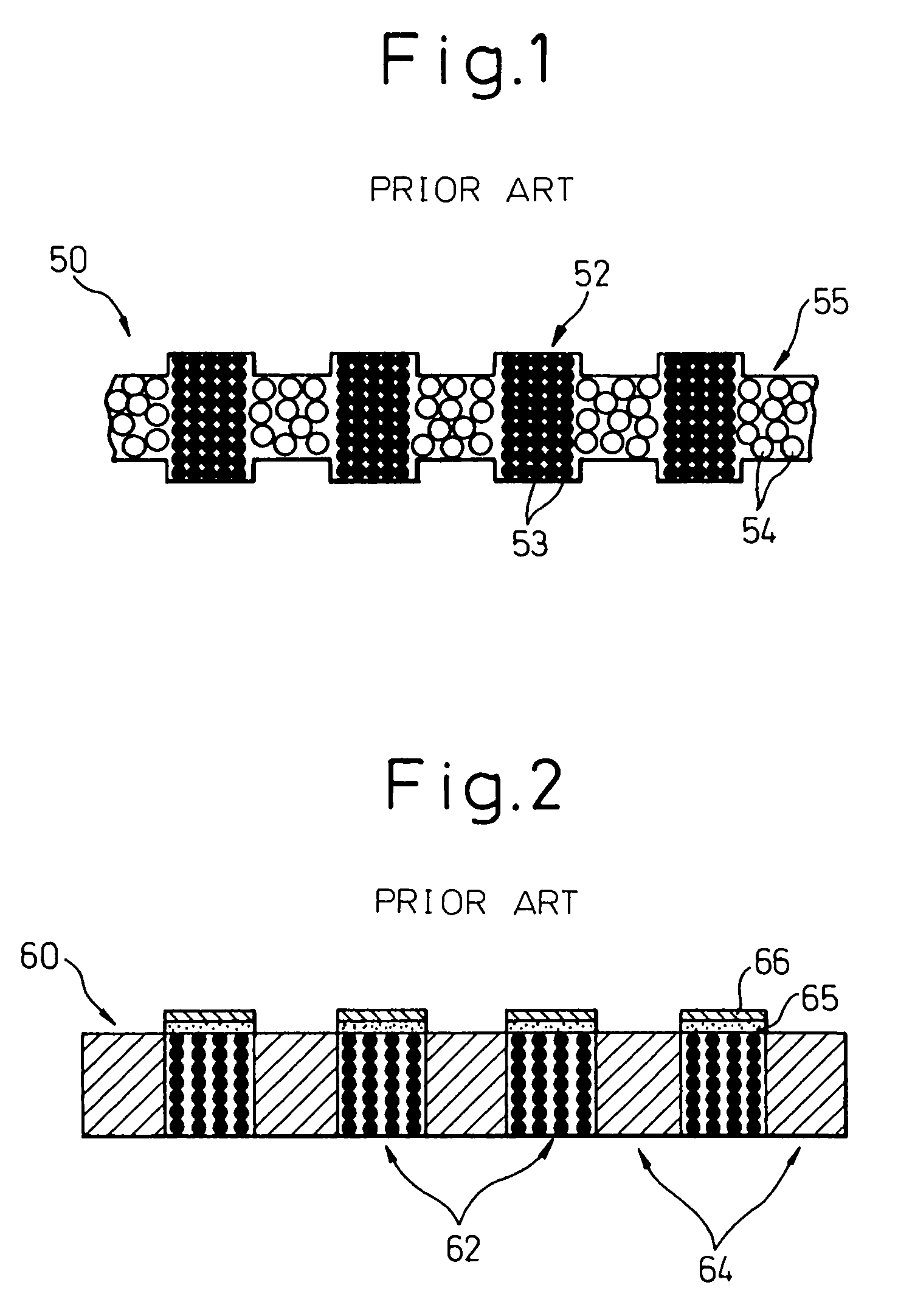
However, the following problems may be encountered in the case of the above anisotropic conductive sheet 60.
Therefore, it is impossible to successfully pierce an aluminum oxide film of which is a protective film for protecting the electrode surface.
Further, the production process is complicated in such a manner that hardening treatment must be conducted under the condition of a parallel magnetic field, which causes an increase in the production cost.

Method used


Image

  • Anisotropic conductive sheet, production process, contact structure, electronic device and inspection apparatus for operation test
  • Anisotropic conductive sheet, production process, contact structure, electronic device and inspection apparatus for operation test
  • Anisotropic conductive sheet, production process, contact structure, electronic device and inspection apparatus for operation test

Examples


example 1

[0119]In this example, an anisotropic conductive sheet was produced by the method explained above referring to FIGS. 15A to 15E.

[0120]As an insulating base material, there was prepared a polyether etherketone film, the thickness of which is 300 μm. At predetermined positions in this base material, through-holes, the diameters of which are 0.2 mm, were formed with a precision drill. Next, a conductive adhesive, which exhibits rubber elasticity after it has been hardened, was charged into the respective through-holes with a spatula in the manner similar to screen printing. (The conductive adhesive used herein was a material the matrix of which is urethane, the hardness of which is substantially identical with 6B of pencil hardness, and which is available as the item number “3302F” from Three Bond Corporation). Immediately after charging, metal covered powders as a contact-forming conductive material were coated on the conductive adhesive layer and heated at 120° C. in an oven for one ...

example 2

[0122]In this example, an anisotropic conductive sheet was produced by the method explained above referring to FIGS. 16A to 16E.

[0123]An insulating base material was made in such a manner that PET films of 100 μm thickness were bonded onto both faces of a polyether etherketone film of 300 μm thickness with a simple peeling adhesive. Through-holes of 0.2 mm diameter were formed at predetermined positions of this base material with a precision drill. Next, a conductive adhesive, which exhibits rubber elasticity after it has been hardened, was charged into the respective through-holes with a spatula in the manner similar to screen printing. (The conductive adhesive used herein was a material the matrix of which is urethane, the hardness of which is substantially identical with 6B of pencil hardness, and which is available as the item number “3303E” from Three Bond Corporation.) Immediately after charging, metal covered powders as contact-forming conductive material were coated on the c...


PUM

PropertyMeasurementUnit
temperaturesaaaaaaaaaa
thicknessaaaaaaaaaa
thicknessaaaaaaaaaa

Abstract

An anisotropic conductive sheet comprising an insulating base material and a plurality of conductive passages embedded at predetermined positions in the insulating base material, penetrating the insulating base material in the thickness direction. The conductive passage comprises a matrix consisting of non-silicone material or silicone material having rubber elasticity, the matrix material being filled into through-holes formed at a predetermined position in the base material and then hardened, and a conductive filler dispersed in the matrix at an amount capable of exhibiting conductivity at all times. A surface layer of conductive material is capable of functioning as a contact and ensuring an electrical connection by piercing a surface layer of an opponent when the surface layer is used as a contact, such as a layer of fine conductive particles is further provided on at least one of the end faces of the conductive passage. An anisotropic conductive sheet of the present invention can be advantageously used in an electronic device or inspection apparatus, used for an operation test, as a contactor.

Description

CROSS-REFERENCE TO RELATED PATENT APPLICATIONS[0001]This patent application is based on Japanese Patent Application No. 2001-140497 filed on May 10, 2001, and claims the priority of this patent application, the contents being incorporated herein by reference.BACKGROUND OF THE INVENTION[0002]1. Field of the Invention[0003]The present invention relates to a contact structure. More particularly, the present invention relates to a contact structure used for the electrical connection of electronic parts represented by LSI, in other words, a contactor. Especially, the present invention relates to an anisotropic conductive sheet used as a contactor in the electrical connection between circuit devices such as electronic parts or used as a contactor in the inspection apparatus used for inspecting the operation of circuit devices such as a printed circuit board and semiconductor integrated circuit. The present invention also relates to an electronic device and inspection apparatus for operati...

Claims


Application Information

Patent Timeline
Patent Type & Authority Patents(United States)
IPC IPC(8): H01R4/58G01R1/067G01R1/073H01R11/01H01B5/16H01B13/00H01R33/76H01R43/00
CPCG01R1/06755G01R1/07314G01R3/00G01R1/07378
Inventor HASHITANI, TAKAFUMIMARUYAMA, SHIGEYUKI
Owner FUJITSU LTD
Why Eureka
Try Eureka