Spin-on glass composition and method of forming silicon oxide layer in semiconductor manufacturing process using the same

a technology of spin-on glass and semiconductor manufacturing, which is applied in the direction of liquid/solution decomposition chemical coating, transportation and packaging, coatings, etc., can solve the problems of uneven surface of the first insulation layer, affecting the stability of the second metal layer, and increasing irregular topography of the top layer

Inactive Publication Date: 2007-09-18
SAMSUNG ELECTRONICS CO LTD
View PDF16 Cites 46 Cited by
  • Summary
  • Abstract
  • Description
  • Claims
  • Application Information

AI Technical Summary

Benefits of technology

[0025]Accordingly, it is a feature of an embodiment of the present invention to provide a spin-on glass composition that fills gaps between closely-spaced metal wirings of semiconductor devices having a high packing density and a large aspect ratio. It is also a feature of the present invention to provide a composition that fills gaps or smoothes surface discontinuities on a substrate without the need for mechanical planarization. It also is a feature of the invention to provide a spin-on glass composition that has substantially the same characteristics as an oxide layer of a semiconductor device formed by a chemical vapor deposition (CVD) method. It is another feature of the invention to provide a method of forming an oxide layer in a semiconductor manufacturing process using the above spin-on glass composition.

Problems solved by technology

In such a multilevel interconnection structure, the topography of the top layer usually is increasingly irregular and uneven as the number of layers increases.
At this time, the surface of the first insulation layer is uneven because the layers underlying the first insulation layer are uneven.
When the second metal layer is directly formed on the first insulation layer, the second metal layer may fracture due to protrusions or cracks in the underlying insulation layer.
In addition, there may be a decreased yield of the semiconductor device if the deposition state of the metal layer is poor.
However, depositing BPSG presents problems because it depends primarily on establishing special deposition parameters for the equipment utilized.
In addition, the gases used in the process are expensive and severely toxic.
Furthermore, as the packing density increases and the design rule gradually decreases for manufacturing VLSI having 256 megabits or more, using BPSG as the insulation layer to fill gaps between wirings lowers the yield due to the occurrence of voids and bridges.
In addition, an etch stop layer may possibly be damaged during its subsequent formation.
Thus, the prior art typically implements a reflowing process and an expensive CMP process to solve these problems.
In addition, because SOG is deposited by a spin coating method, the thickness of the thus formed silicon oxide layer is not sufficient.
This provides insufficient coverage for the conductive layers, such as gate electrodes and metal wirings.
The generation of the oxide might induce a shape defect at a dent portion after implementing a CMP process or might change the size of the active region.

Method used


Image

  • Spin-on glass composition and method of forming silicon oxide layer in semiconductor manufacturing process using the same
  • Spin-on glass composition and method of forming silicon oxide layer in semiconductor manufacturing process using the same
  • Spin-on glass composition and method of forming silicon oxide layer in semiconductor manufacturing process using the same

Examples


example 1

[0090]Preparation of an SOG Composition

[0091]Perhydropolysilazane having a weight average molecular weight of 4,500-7,000 and a molecular weight dispersion degree of 3.0-4.0 was obtained by fractionating commercially available perhydropolysilazane. The fractionated perhydropolysilazane was dissolved in xylene to obtain an SOG composition having a perhydropolysilazane concentration of 22-25% by weight, based on the total weight of the composition. The contact angle of the SOG composition was 4° or less with respect to an underlying silicon nitride layer.

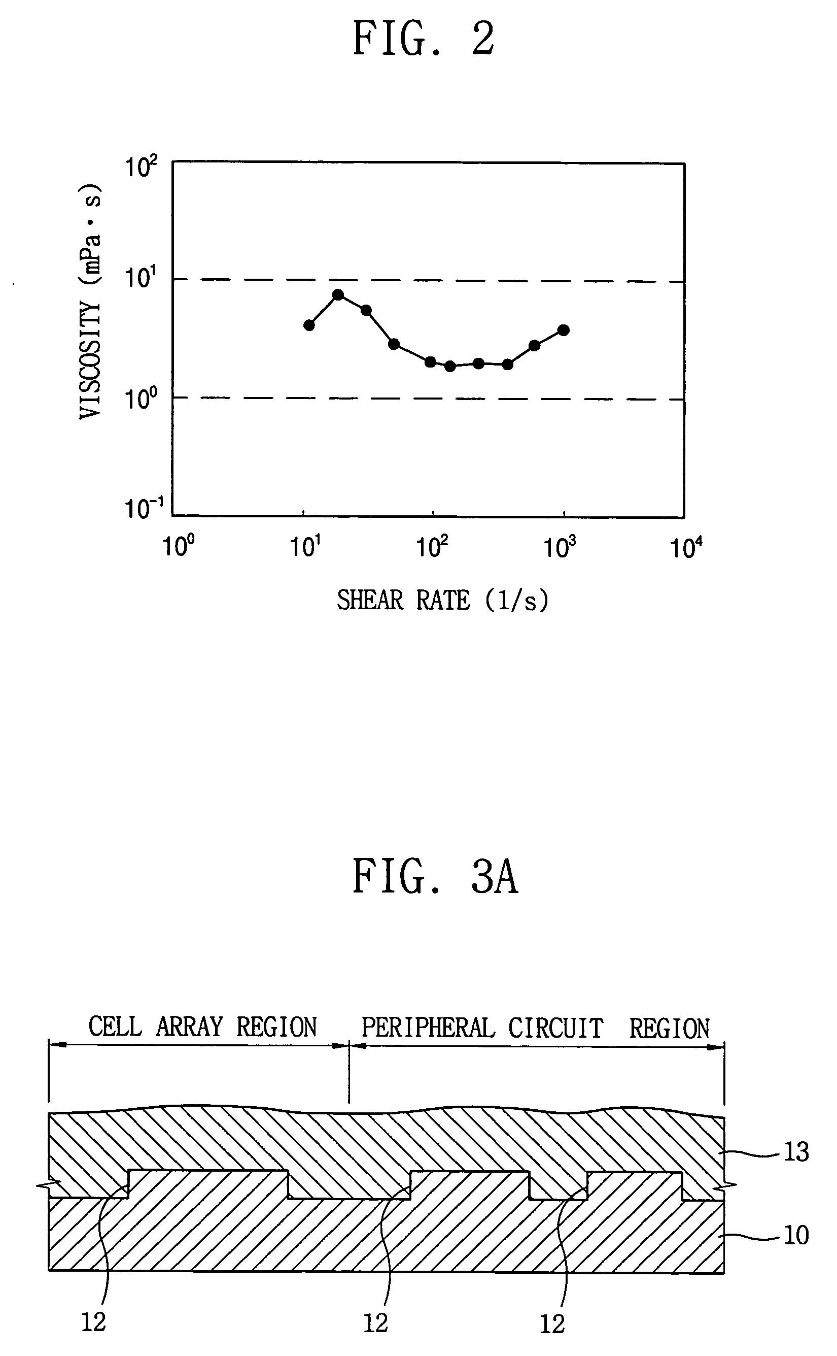
[0092]The viscosity of the SOG composition was detected according to the variation of its shear rate. The viscosity characteristic is illustrated in FIG. 2. FIG. 2 is a graph illustrating the viscosity change with respect to the shear rate change of the SOG solution. The ordinate represents the viscosity (mPa.s) and the abscissa represents the shear rate (1 / s). As can be seen in FIG. 2, the SOG solution preferably has a uniform viscos...

example 2

[0132]Preparation of an SOG Composition

[0133]Referring to FIG. 7F, thus formed silicon oxide layer 214 was polished by a CMP method until the polishing stopping layer 204 on the semiconductor substrate 200 was exposed. Then, the inner portion of the trench 210 was buried with silicon oxide 214. Reference numeral 216 refers to a silicon oxide layer filling the trench.

[0134]Shallow Trench Isolation

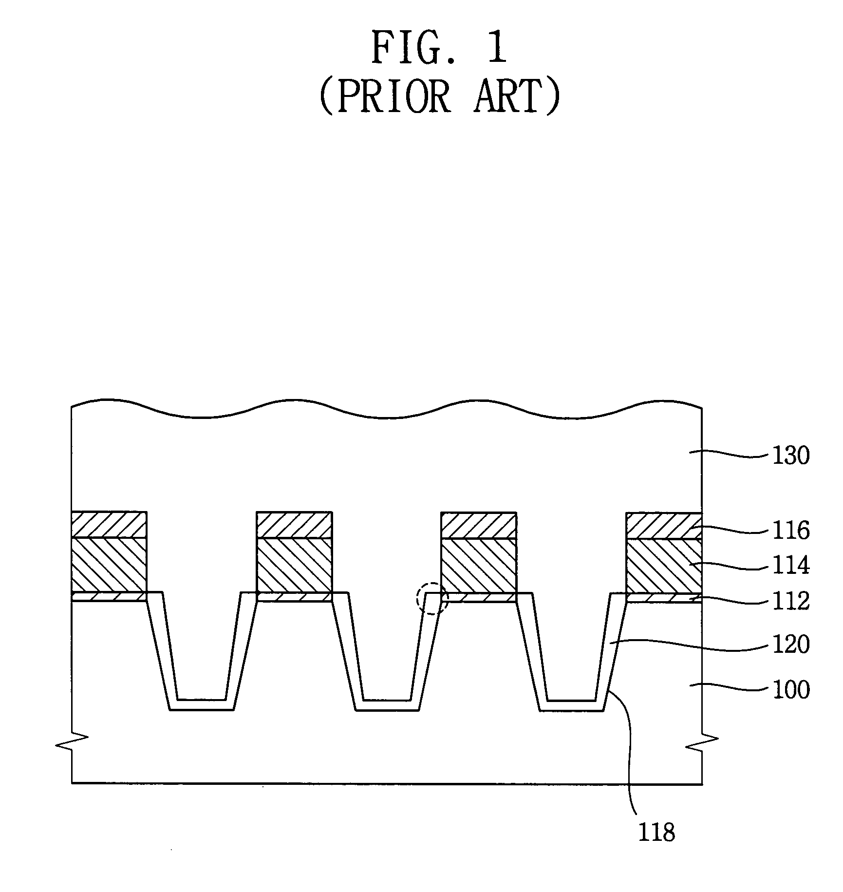
[0135]When the field oxide 14 illustrated in FIG. 3 is formed to bury the trench of the highly integrated semiconductor device according to Example 1, a thick oxide layer is formed at the inner wall of the trench as illustrated in FIG. 1.

[0136]FIGS. 7A-7G are cross-sectional views for illustrating an isolating method of a shallow trench device according to further another embodiments of the present invention.

[0137]Referring to FIG. 7A, a pad oxide layer 201 having a thickness of about 100-200 Å was formed by a thermal oxidation process on a semiconductor substrate made of silicon. Then, a ni...

example 3

[0181]Preparation of an SOG Composition

[0182]Perhydropolysilazane having a weight average molecular weight of 3,000-6,000 and a molecular weight dispersion degree of 2.5-3.5 was obtained by fractionating commercially available perhydropolysilazane. The fractionated perhydropolysilazane was dissolved in xylene to obtain an SOG composition having a perhydropolysilazane concentration of 20-23% by weight, based on the total weight of the composition. The contact angle of the SOG composition was 4° or less with respect to an underlying silicon nitride layer.

[0183]The viscosity of the SOG composition was detected according to the variation of its shear rate. The SOG solution preferably has a uniform viscosity within the range of about 1.54 to 1.70 cP.


PUM

PropertyMeasurementUnit
viscosityaaaaaaaaaa
contact angleaaaaaaaaaa
temperatureaaaaaaaaaa

Abstract

A spin-on glass (SOG) composition and a method of forming a silicon oxide layer utilizing the SOG composition are disclosed. The method includes coating on a semiconductor substrate having a surface discontinuity, an SOG composition containing polysilazane having a compound of the formula —(SiH2NH)n— wherein n represents a positive integer, a weight average molecular weight within the range of about 3,300 to 3,700 to form a planar SOG layer. The SOG layer is converted to a silicon oxide layer with a planar surface by curing the SOG layer. Also disclosed is a semiconductor device made by the method.

Description

CROSS-REFERENCE OF RELATED APPLICATIONS[0001]This application is a Continuation-in-part application of “METHOD OF FORMING SILICON OXIDE LAYER IN SEMICONDUCTOR MANUFACTURING PROCESS USING SPIN-ON GLASS COMPOSITION AND ISOLATION METHOD USING THE SAME METHOD”, by the present inventors, Ser. No. 10 / 278,992, filed on Oct. 24, 2002 now U.S. Pat. No. 7,179,537, which itself is a Continuation-in-part application of “SPIN-ON GLASS COMPOSITION AND METHOD OF FORMING SILICON OXIDE LAYER IN SEMICONDUCTOR MANUFACTURING PROCESS USING THE SAME”, by the present inventors, Ser. No. 09 / 686,624, filed on Oct. 12, 2000 now U.S. Pat. No. 6,706,646, the contents of both of which are herein incorporated by reference in their entirety. This application also relies for priority upon Korean Patent Application No. 2003-79508, filed Nov. 11, 2003, the contents of which are herein incorporated by reference in their entirety.BACKGROUND OF THE INVENTION[0002]1. Field of the Invention[0003]The present invention rel...

Claims


Application Information

Patent Timeline
Patent Type & Authority Patents(United States)
IPC IPC(8): B32B7/02C08L83/00H01L21/316C23C18/12H01L21/3105H01L21/312H01L21/314H01L21/762H01L21/768H01L21/8239H01L21/8242
CPCC09D183/16C23C18/06C23C18/1212C23C18/122C23C18/1275C23C18/1279C23C18/1283H01L21/02126H01L21/02129H01L21/02164H01L21/02282H01L21/02337H01L21/31051H01L21/3125H01L21/316H01L21/31612H01L21/76229H01L21/76826H01L21/76828H01L21/76829H01L21/76837H01L27/10882H01L27/10894H01L27/1052Y10T428/31663H10B99/00H10B12/48H10B12/09
Inventor LEE, JUNG-HOCHO, JUN-HYUNCHOI, JUNG-SIKLEE, DONG-JUN
Owner SAMSUNG ELECTRONICS CO LTD
Why Eureka
Try Eureka