
Neutron detection device and method of manufacture

a technology of neutron detection and manufacturing method, which is applied in the direction of material analysis, measurement with semiconductor devices, instruments, etc., can solve the problems of false positives, helium-3 filled tubes are delicate, and require careful handling, and achieve low power consumption, increase the sensitivity of the neutron detection device, and the effect of inexpensive design and manufactur

Inactive Publication Date: 2007-09-18
THE UNITED STATES OF AMERICA AS REPRESENTED BY THE SECRETARY OF THE NAVY
View PDF5 Cites 36 Cited by
  • Summary
  • Abstract
  • Description
  • Claims
  • Application Information

AI Technical Summary

Benefits of technology

The invention is a neutron detection device that is sensitive, low-powered, and can detect single neutron events. It does not require high pressure tubes or high voltages for operation and is not affected by gamma rays or thermal noise. The device can be manufactured at a low cost and can be modified from existing semiconductor memory devices. It includes a layer of charge-sensitive semiconductor elements and a layer of neutron conversion material close to the semiconductor elements. The close proximity of the neutron conversion layer to the semiconductor elements increases sensitivity. The device can be constructed from a conventional SRAM memory device by removing the base substrate and forming a neutron conversion layer on the insulating layer.

Problems solved by technology

In particular, the helium-3 filled tubes are delicate, require careful handling, and can indicate false positives when abruptly moved or struck.
These types of conventional neutron detectors are effective in many types of field operations, but they are not suitable for operations requiring compact and highly sensitive devices capable of functioning for long periods of time with low power consumption.
Lithium metal has been used for this purpose, although the chemical reactivity of the lithium metal leads to shorter detector life.
The use of diode structures in neutron detectors, however, has its own set of drawbacks and limitations.
The internal noise level of an uncooled diode is appreciable, and consequently it is difficult, if not impossible, to measure low background levels of ambient thermal neutrons in the surrounding area or to detect single neutron events.
A radiation-induced bit error is known as a soft error if the affected memory cell subsequently responds to write commands.
In contrast, the induced bit error is known as a hard error if subsequent attempts to change the state of the memory cell are ineffective.
These efforts to date, however, have resulted in insensitive detectors primarily because the boron conversion material is not located close enough to the active semiconductor layer.
Thus, alpha particles generated by the boron conversion material dissipate their energy in the intervening material and cannot generate a sufficient charge in the active semiconductor layer to cause an SEU.

Method used


Image

  • Neutron detection device and method of manufacture
  • Neutron detection device and method of manufacture
  • Neutron detection device and method of manufacture

Examples


Embodiment Construction

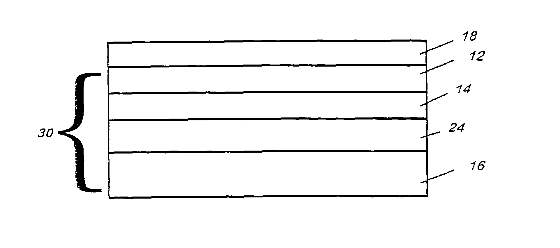
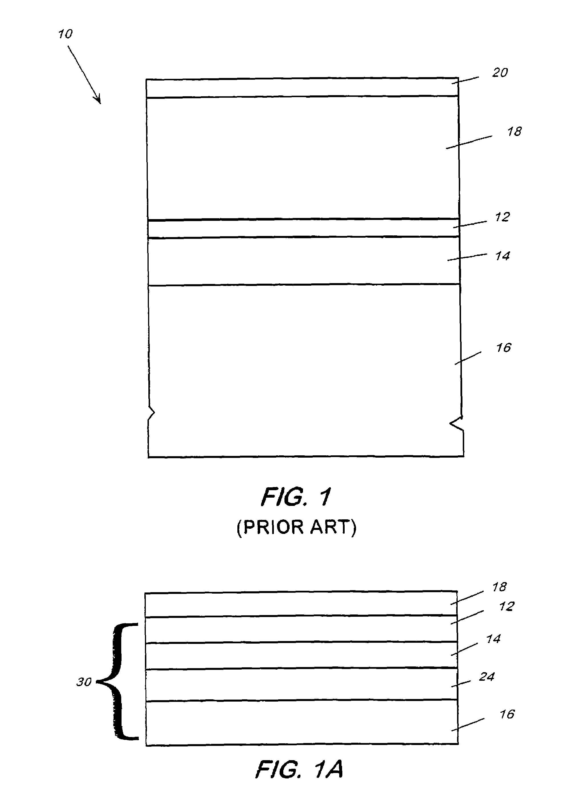
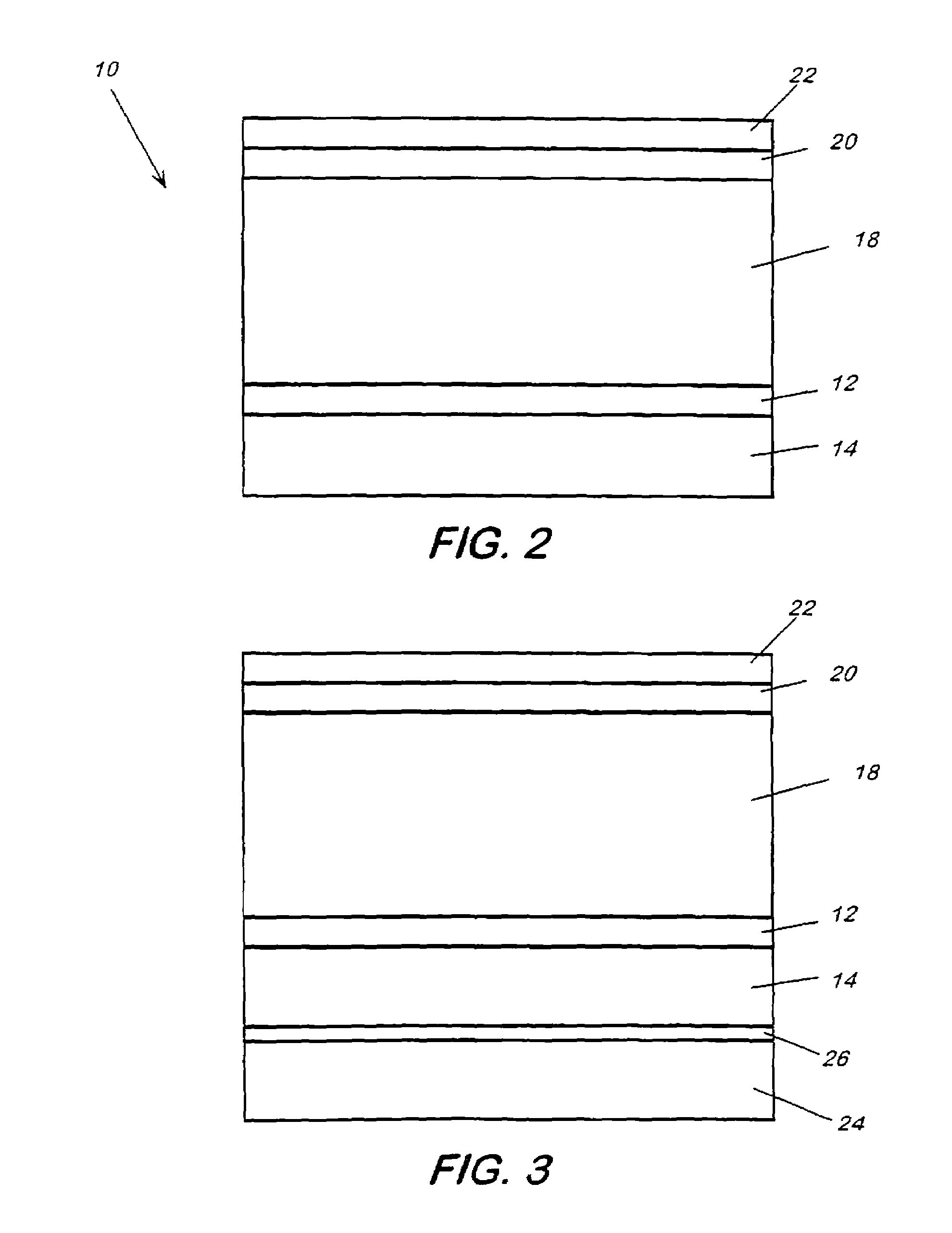
[0028]This application hereby incorporates by reference the application entitled “Semiconductor Substrate Incorporating a Neutron Conversion Layer”, filed on date even herewith, now issued at U.S. Pat. No. 6,867,444. The present invention is directed to a neutron detection device that utilizes a neutron conversion layer in close proximity to charge-sensitive elements such as conventional memory cells. Specifically, the device provides a neutron conversion layer in close proximity to the active semiconductor layer of a charge-sensitive electronic semiconductor device such as a semiconductor memory cell. In particular, the invention will be described with reference to an SRAM memory device formed on a SOI substrate. It will be understood, however, that the invention is not limited to the specifically disclosed embodiment disclosed with reference to silicon devices but may also be realized with other semiconductor materials, and that alpha-emitting neutron converters based on boron and...


PUM


Abstract

A neutron detection device includes a neutron conversion layer in close proximity to an active semiconductor layer. The device is preferably based on the modification of existing conventional semiconductor memory devices. The device employs a conventional SRAM memory device that includes an SOI substrate. The SOI substrate includes an active semiconductor device layer, a base substrate and an insulating layer between the active semiconductor device layer and the base substrate. The base substrate layer is removed from the memory device by lapping, grinding and / or etching to expose the insulating layer. A neutron conversion layer is then formed on the insulating layer. The close proximity of the neutron conversion layer to the active semiconductor device layer yields substantial improvements in device sensitivity.

Description

BACKGROUND OF THE INVENTION[0001]The present invention is directed in general to a neutron detection device and a method of manufacturing a neutron detection device. The present invention is specifically directed to a semiconductor device for the detection of neutrons that utilizes a neutron conversion layer in close proximity to a conventional memory cell structure.[0002]The development of nuclear weapons gave rise to several urgent applications for highly sensitive neutron detectors. The applications included safeguarding nuclear materials and weapons, treaty verification, anti-proliferation, and the recovery of lost military payloads. More recently, however, the need to guard against nuclear smuggling, the potential of a radiological weapon (so called “dirty” bombs), and terrorist acts, has given rise to an urgent need to perform neutron surveillance at border and port facilities, transportation systems and other places where large amounts of a cargo or people pass by or through ...

Claims


Application Information

Patent Timeline
Patent Type & Authority Patents(United States)
IPC IPC(8): G01T3/08H01L31/115
CPCG01T3/08H01L31/115
Inventor AUGUST, ROBERT A.HUGHES, HAROLD L.MCMARR, PATRICK J.WHITLOCK, ROBERT R.
Owner THE UNITED STATES OF AMERICA AS REPRESENTED BY THE SECRETARY OF THE NAVY
Learn More