MgO-based tunnel spin injectors

a tunnel junction and injector technology, applied in the direction of superconductor devices, electrical apparatus, semiconductor devices, etc., can solve the problems of low injection efficiency of ferromagnetic metals into semiconductors through diffusive contacts, weak temperature dependence of the tunneling process. , to achieve the effect of high spin polarization of injected electrons, good thermal stability and low cos

Inactive Publication Date: 2007-09-25
IBM CORP
View PDF59 Cites 101 Cited by
  • Summary
  • Abstract
  • Description
  • Claims
  • Application Information

AI Technical Summary

Benefits of technology

[0011]The present invention provides a MgO based tunnel spin injector as a source of highly spin-polarized electrons at useful temperatures for semiconductor spintronic applications. The spin injector includes a ferromagnetic metal electrode and a MgO tunnel barrier grown on a semiconductor. By applying a bias voltage across the entire structure, spin-polarized electrons can be transported into the semiconductor for further spin manipulation and detection. The spin injector of the present invention has many advantages over prior art spin injectors including the high spin polarization of the injected electrons at room temperature and good thermal stability. A lower bound for spin injection efficiency of ˜50% is observed at 100 K, which is expected to remain high up to room temperature due to the high Curie temperatures of the ferromagnetic metals and the weak temperature dependence of the tunneling process.
[0013]The present invention also provides a method of improving the spin injection efficiency by thermal annealing. The thermal annealing, in addition, provides evidence that good thermal stability is achieved in the present invention.
[0019]A preferred method of forming the MgO tunnel barrier on the underlayer includes depositing Mg onto a surface of the underlayer to form a Mg layer thereon (in which the surface is selected to be substantially free of oxide). The preferred method further includes directing additional Mg, in the presence of oxygen, towards the Mg layer to form a MgO tunnel barrier in contact with the underlayer, in which the oxygen reacts with the additional Mg and the Mg layer. The thickness of the Mg layer is preferably selected to be large enough to prevent oxidation of the underlayer but small enough that, upon reaction of the oxygen with the Mg layer, substantially all the Mg in the Mg layer is converted into MgO; the Mg layer, however, is preferably deposited in the absence of substantial amounts of reactive oxygen. The resulting MgO tunnel barrier advantageously has a thickness of between 3 and 50 angstroms. The method preferably further includes annealing MgO tunnel barrier to improve its tunneling characteristics.

Problems solved by technology

However, as the device minimum feature size shrinks towards fundamental physical limits, which will eventually preclude or slow down scaling to even smaller sizes, there are increasing efforts to search for alternatives to conventional electronic devices.
However, a major obstacle for semiconductor spintronics is the electrical generation of highly spin-polarized carriers within semiconductors, which is often referred to as spin injection.
However, despite considerable effort over many years the efficiency of spin injection from ferromagnetic metals into semiconductors through diffusive contacts has been determined experimentally to be very low [see, for example, Filip et al., Physical Review B 62, 9996 (2000)].
While for a long time this was regarded as a problem of spin relaxation within the ferromagnet / semiconductor contact region, perhaps due to the poor structural integrity of such contacts, it is now believed that the injection efficiency is fundamentally limited by the mismatch in conductivity between typical ferromagnetic metals and semiconductors [Schmidt et al., Physical Review B 62, R4790 (2000)].
Furthermore, to grow the Fe layer 32 with MBE is impractical for device fabrication.
The direct contact of the Fe layer 32 with the semiconductor LED 11 could cause intermixing between the two and thus compromise the device thermal stability.
The directly measured light polarization was only a few percent at 80 K, and the interpretation of the data could be further complicated by other parasitic effects.
Thus none of these prior art spin injectors give significant spin-polarized electrons at room temperature.

Method used


Image

  • MgO-based tunnel spin injectors
  • MgO-based tunnel spin injectors
  • MgO-based tunnel spin injectors

Examples


Embodiment Construction

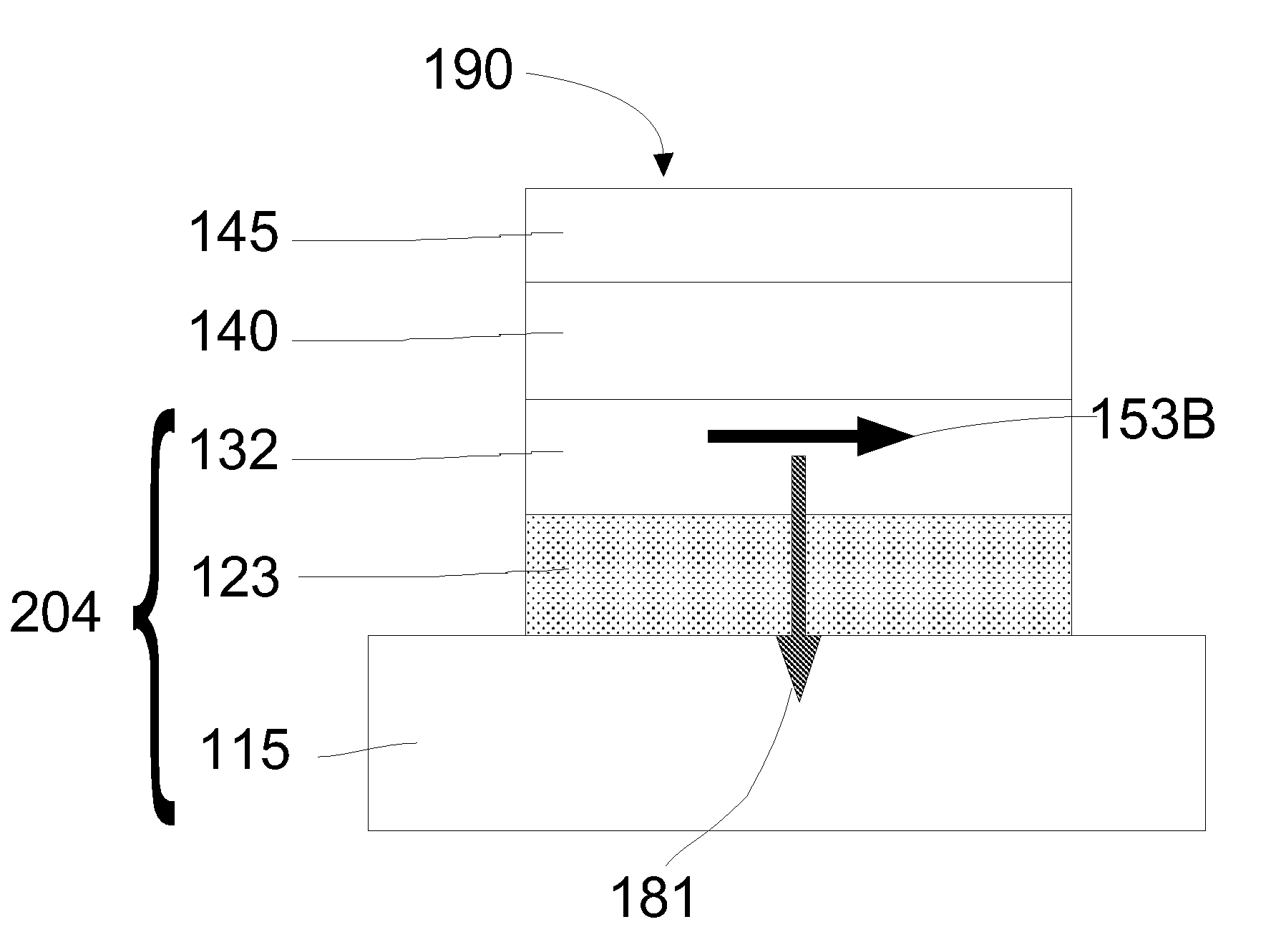
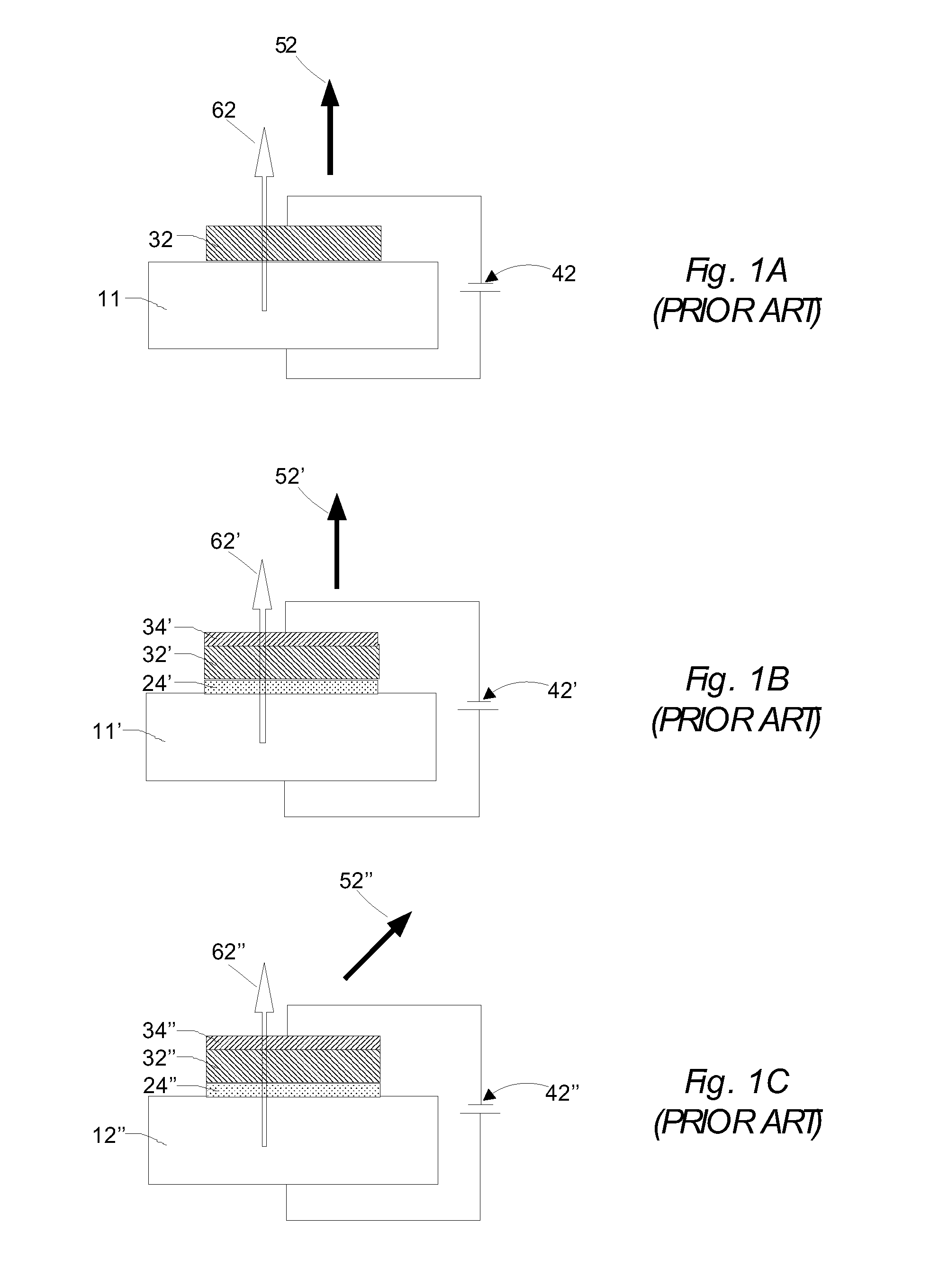
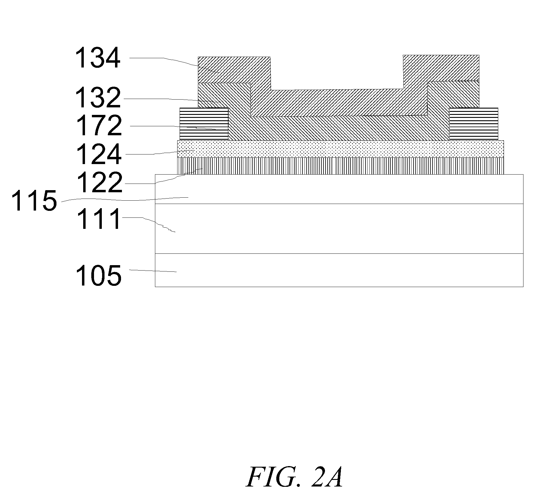
[0038]Theoretical calculations have predicted that tunneling structures based on crystalline MgO tunnel barriers can have much higher tunneling spin polarization compared to conventional tunneling structures based on amorphous Al2O3 tunnel barriers [Butler et al., Physical Review B 63, 054416 (2001); Mathon and Umerski, Physical Review B 63, 220403(R) (2001)]. However, prior art methods used to deposit MgO tunnel barriers have shown low tunneling spin polarization values most likely because of ferromagnetic oxides formed at the interface between the MgO tunnel barrier and the ferromagnetic layers. There have been several studies on the epitaxial growth of MgO onto GaAs substrates as buffer layers for the growth of superconducting or ferroelectric films. These prior art methods of forming MgO layers on GaAs include pulsed laser deposition, electron beam evaporation and magnetron sputtering of MgO layers directly onto GaAs or passivated GaAs surfaces. For example Bruley et al. [Appl. ...


PUM


Abstract

A MgO tunnel barrier is sandwiched between semiconductor material on one side and a ferri- and / or ferromagnetic material on the other side to form a spintronic element. The semiconductor material may include GaAs, for example. The spintronic element may be used as a spin injection device by injecting charge carriers from the magnetic material into the MgO tunnel barrier and then into the semiconductor. Similarly, the spintronic element may be used as a detector or analyzer of spin-polarized charge carriers by flowing charge carriers from the surface of the semiconducting layer through the MgO tunnel barrier and into the (ferri- or ferro-) magnetic material, which then acts as a detector. The MgO tunnel barrier is preferably formed by forming a Mg layer on an underlayer (e.g., a ferromagnetic layer), and then directing additional Mg, in the presence of oxygen, towards the underlayer.

Description

[0001]This application is a continuation-in-part of, and claims priority to, Applicant's application Ser. No. 10 / 646,247 filed Aug. 22, 2003 now abandoned and entitled “MgO-Based Tunnel Spin Injectors”, which is hereby incorporated by reference.[0002]The U.S. Government has a paid-up license in this invention and the right in limited circumstances to require the patent owner to license others on reasonable terms as provided for by the terms of contract MDA972-01-C-0051 awarded by DARPA.TECHNICAL FIELD[0003]This invention relates to tunnel junction injectors and detectors of spin-polarized electrons for use in semiconductor spintronic devices. More particularly, this invention relates to a tunnel injector with high spin polarization formed from a ferromagnetic layer in conjunction with a MgO tunnel barrier on a semiconductor.BACKGROUND OF THE INVENTION[0004]The development of modern semiconductor electronics has followed Moore's law [G. E. Moore, Electronics 38, 114 (1965)] for sever...

Claims


Application Information

Patent Timeline
Patent Type & Authority Patents(United States)
IPC IPC(8): H01L21/00H01L29/82
CPCH01L29/66984Y10S977/933
Inventor PARKIN, STUART STEPHEN PAPWORTH
Owner IBM CORP
Why Eureka
Try Eureka