Advanced pattern definition for particle-beam processing

a technology of advanced pattern definition and particle beam, which is applied in the direction of beam deviation/focusing by electric/magnetic means, treatment, and beam handling using diaphragms/collimeters, etc. it can solve the problems of insufficient number of gray scale levels in single pass exposures, complex internal structure, and prone to unwanted disturbing effects, so as to improve resolution and reduce line edge roughness , the effect of unchanged

Active Publication Date: 2007-10-02
IMS NANOFABTION
View PDF8 Cites 167 Cited by
  • Summary
  • Abstract
  • Description
  • Claims
  • Application Information

AI Technical Summary

Benefits of technology

[0021]In view of the above, it is the task of the present invention to find a way to overcome the deficiencies of prior art and allow the use of an addressable mask for applications such as mask-less lithography or nano-scale beam patterning applications. A central aim is to enhance the resolution that can be obtained with a PD device, realizing a finer address grid and reducing the line edge roughness despite an unchanged or even reduced number of apertures compared to prior art. Furthermore, it shall allow the irradiation of pixels at the target according to a gray scale, i.e. with exposure levels interpolated between a minimal (‘black’) and maximal (‘white’) exposure dose.
[0024]On account of the invention a finer resolution is available on the target surface even though the individual spots formed by each image of an individual aperture are not decreased in size. Furthermore, the invention enables a downscaling of the lithographic node, for example from 45 mn to 32 nm lines and spaces resolution, without simultaneously downscaling the critical dimensions in the PD device. Hence, the invention helps to circumvent the feature size limitation of state-of-the-art MEMS technology. All together, the invention allows to significantly reduce the diameter of the optical beam and the required PD device in PML2 with the purpose to relax optical performance requirements, such as for example the absence of distortion, and to improve productivity by using several columns in parallel.
[0028]In a preferred embodiment of the invention the group blanking signals are fed to the PD field partly at a side running parallel to the orientation of lines, partly at a side running perpendicular. This further reduces the density of lines at the feeding sites.
[0029]In a suitable realization of the aperture arrangement, the shape of the apertures is substantially equivalent to a two-dimensional geometrical base shape of a contiguous covering of the plane, such as a square or a regular hexagon. The advantage of a contiguous covering arrangement is that the influence of the optical imaging blur on the dose distribution on the wafer (=aerial image), in particular on the gray levels needed for a specific feature, is as small as possible, so that an intrinsic radial variation of the optical imaging blur inside the projected image of the PD device can be tolerated. If the blur is in the range of the spot size, the same advantage can be achieved by choosing the area of the apertures substantially equivalent to a two-dimensional geometrical base shape of a contiguous covering of the plane, whereas the shape may differ from that of a contiguous covering, in particular by modifying the edges of a polygonal base shape such as rounding the edges or beveling (canting). The total shape should be enlarged, if necessary, so the total area of the modified shape is kept, and the area of the shape of the apertures is the same as that of the original polygonal base shape. This means, for example, that instead of perfectly square-shaped apertures it is possible to use corner-rounded square shaped apertures with equal area. The latter allows higher tolerances in the fabrication process. In general, a hexagonal arrangement has the advantage that it has the highest possible density of pixels per area combined with the highest degree of symmetry, both improving the achievable line placement precision and line edge roughness at limited number of apertures in the PD means (=limited size of the PD field).

Problems solved by technology

Yasuda et al., U.S. Pat. No. 5,359,202 and U.S. Pat. No. 5,260,579 use a similar BAA for exposing a substrate with a pattern, but the need to fed control lines to each of the blanking apertures makes the internal structuring very complex and prone to unwanted disturbing effects such as cross-talking and transit time delays.
However, with the PLM2 layout, like with other prior art, the following main problems arise:using the physical address grid available by the BAA of prior art, in particular Arai et al. and Berry et al., only an insufficient number of gray scale levels is achieved in single pass exposures in order to fulfill lithographic requirements (1 nm address grid for 45 nm node), as the size of the PD field is limited in large field projection systems.
The consequences are a poor process latitude, untolerable values for the line edge roughness, which is related to the physical address grid, and insufficient pattern placement accuracy, or in case of a multi pass strategy, reduced throughput and unwanted alignment errors.the need for a distortion-free imaging of a large pattern field as a consequence to the requirement to bring thousands of apertures in overlay during the scanning process (to exploit the high redundancy); anddealing with an unavoidable current dependent (=pattern dependent) image distortion and de-focusing, limiting the usable current and requiring pattern homogenization, which will involve a time consuming data pre-processing.

Method used


Image

  • Advanced pattern definition for particle-beam processing
  • Advanced pattern definition for particle-beam processing
  • Advanced pattern definition for particle-beam processing

Examples


Embodiment Construction

Pattern Definition System

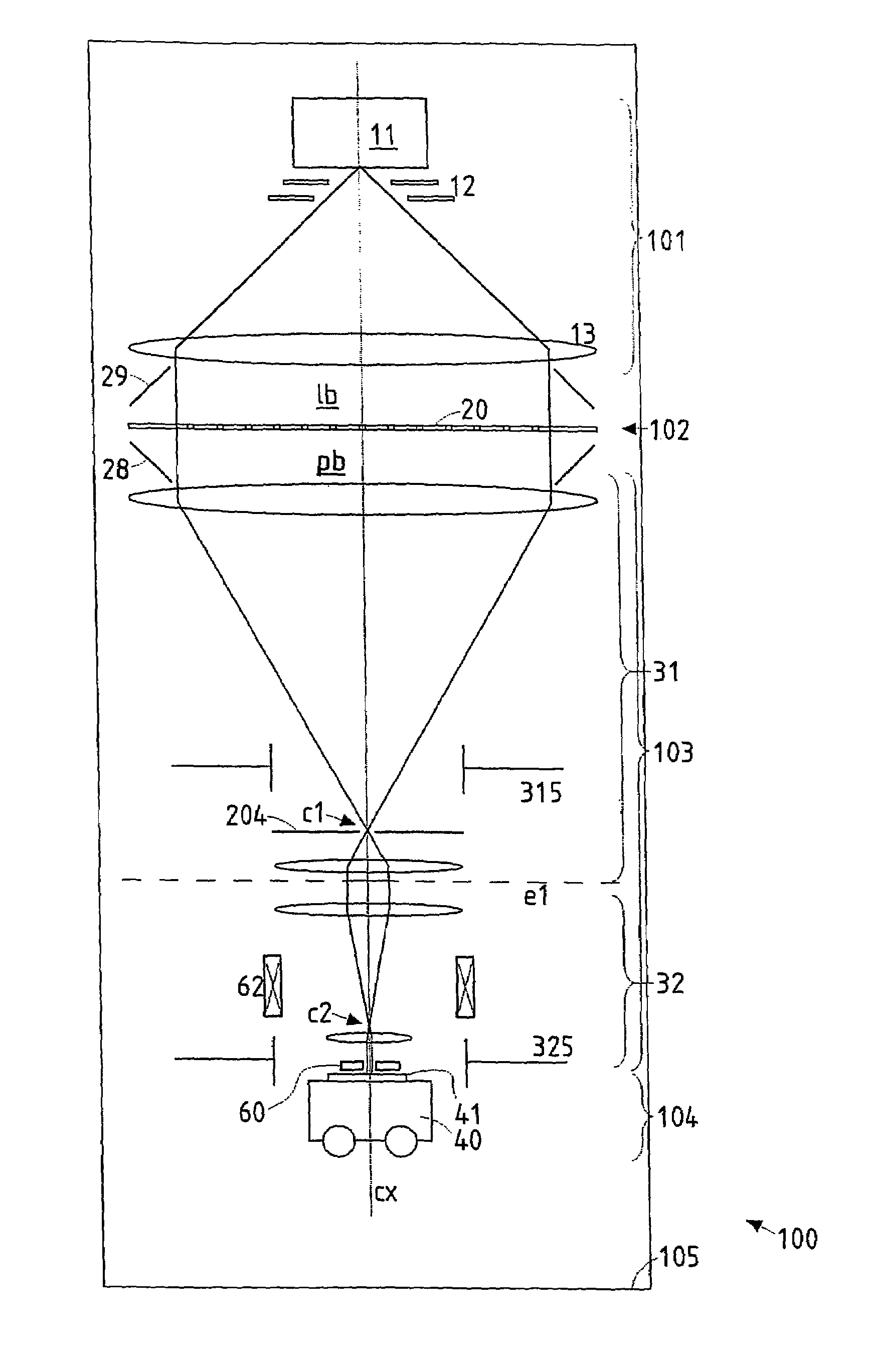
[0050]The preferred embodiments of the invention discussed in the following are based on the pattern definition (PD) system disclosed in the U.S. Pat. No. 6,768,125, used in a ion-beam processing apparatus. In the following, the technical background of the PD system, as far as relevant to the invention, is first discussed with reference to FIGS. 1 to 5 (which correspond, with modifications where appropriate, those of the U.S. Pat. No. 6,768,125), then embodiments of the invention in the PD system are discussed. It should be appreciated that the invention is not restricted to the following embodiments, which merely represent some of the possible implementations of the invention.

[0051]An overview of a processing apparatus employing the preferred embodiment of the invention is shown in FIG. 1. In the following, only those details are given as needed to disclose the invention; for the sake of clarity, the components are not shown to size in FIG. 1. The main comp...


PUM

PropertyMeasurementUnit
side lengthaaaaaaaaaa
sizeaaaaaaaaaa
sizeaaaaaaaaaa

Abstract

In a pattern definition device for use in a particle-beam processing apparatus a plurality of apertures (21) are arranged within a pattern definition field (pf) wherein the positions of the apertures (21) in the pattern definition field (pf) taken with respect to a direction (X, Y) perpendicular, or parallel, to the scanning direction are offset to each other by not only multiple integers of the effective width (w) of an aperture taken along said direction, but also multiple integers of an integer fraction of said effective width. The pattern definition field (pf) may be segmented into several domains (D) composed of a many staggered lines (pl) of apertures; along the direction perpendicular to the scanning direction, the apertures of a domain are offset to each other by multiple integers of the effective width (w), whereas the offsets of apertures of different domains are integer fractions of that width.

Description

CROSS-REFERENCE TO RELATED APPLICATIONS[0001]This application claims the benefit of Austrian Patent Application Serial Nos. A 755 / 2004, filed 30 Apr. 2004 and A 1492 / 2004, filed 6 Sep. 2004FIELD OF THE INVENTION AND DESCRIPTION OF PRIOR ART [0002]The invention relates to improvements of a multi-beam pattern definition device for use in a particle-beam processing apparatus.[0003]More in detail, the invention relates to a pattern definition device for use in a particle-beam processing apparatus, which device is adapted to be irradiated with a beam of electrically charged particles and allow passage of the beam only through a plurality of apertures which are of identical shape and define the shape of beamlets permeating them; the apertures are arranged within a pattern definition field according to a specific arrangement for defining the pattern on a target; with said apertures are associated corresponding blanking openings located such that each of the beamlets traverses that blanking...

Claims


Application Information

Patent Timeline
Patent Type & Authority Patents(United States)
IPC IPC(8): G21K5/10G03F7/20G21K1/04G21K1/08G21K5/04H01J37/04H01J37/08H01J37/30H01J37/305H01J37/317H01L21/027
CPCB82Y10/00B82Y40/00H01J37/045H01J37/3174G21K1/08H01J2237/31774H01J37/3177
Inventor PLATZGUMMER, ELMARCERNUSCA, STEFAN
Owner IMS NANOFABTION
Why Eureka
Try Eureka