Semiconductor device

a technology of semiconductor substrates and semiconductors, applied in the direction of semiconductor integrated circuits, basic electric elements, electrical appliances, etc., can solve the problems of large error between the pattern dimension in the layout design and the actual pattern dimension of the semiconductor substrate, and the delay time of the propagation delay time in the design of the semiconductor integrated circuit, so as to prevent simplify the structure. , the effect of suppressing the variation of the gate length

Active Publication Date: 2007-10-09
GK BRIDGE 1
View PDF6 Cites 124 Cited by
  • Summary
  • Abstract
  • Description
  • Claims
  • Application Information

AI Technical Summary

Benefits of technology

[0012]The object of the present invention is to provide a structure of a semiconductor device which can suppress variations in gate length caused by an optical proximity effect and realize an LSI having high performance even in a miniaturization process.
[0014]According to the present invention, the gate conductor film has no reflex angle in the plan geometry. This provides a semiconductor device which can suppress variations in the gate length of a MIS transistor caused by the optical proximity effect.
[0015]In the case where a plurality of gate conductor films are provided on a single diffusion region, a plurality of gate contacts are provided so as to be in contact with gate interconnect parts, respectively, and an interconnect in contact with the plurality of gate contacts is provided. Thus, the semiconductor device achieves the same function as the MIS transistor having a comb gate while preventing the variations in the gate length of the MIS transistor which would be caused by the optical proximity effect in the known comb gates.
[0016]Moreover, in the case where the plurality of gate conductor films are provided on a single diffusion region, a common gate contact extending across the gate interconnect parts is used as the gate contact, thereby simplifying the structure.
[0018]In the semiconductor device of the present invention, a conductor pad having a larger plane area than the gate contact may be further provided on each gate interconnect part to bring the gate contact into contact with the conductor pad. According to this structure, in forming a gate contact hole and source / drain contact holes simultaneously, the gate contact hole can be prevented from reaching the element isolation region.
[0019]As mentioned above, according to the present invention, it is possible to suppress variations in gate length of various MIS transistors caused by the generation of the optical proximity effect in the photolithographic step of the MIS transistors. As a result, the design margin can be reduced, and hence the LSI having high performance can be provided.

Problems solved by technology

Main factors causing variations in propagation delay time in a design of a semiconductor integrated circuit (LSI) include variations in operating power supply voltage, temperature, process, etc.
As a result, the variations in propagation delay time have also widened and the design margin has increased, and thereby it has become difficult to provide the LSI having high performance.
In the exposure of the photolithographic step, if the pattern dimension is not more than the exposure wavelength, the optical proximity effect generated by the influence of diffracted light causes a large error between the pattern dimension in the layout design and the actual pattern dimension on the semiconductor substrate.
However, the optical proximity effect inevitably occurs, and it is difficult to prevent the optical proximity effect only by manufacturing and process techniques such as the super resolution technique and the OPC technique.
In this case, a reflex angle at the boundary between the pad and the gate interconnect part is rounded due to the optical proximity effect, which causes errors in the dimension of the gate electrode part provided on the active region, namely in the gate length of the transistor.
However, this increases the area of the semiconductor device, decreases integration density, and hence is not practical.

Method used


Image

  • Semiconductor device
  • Semiconductor device
  • Semiconductor device

Examples


first embodiment

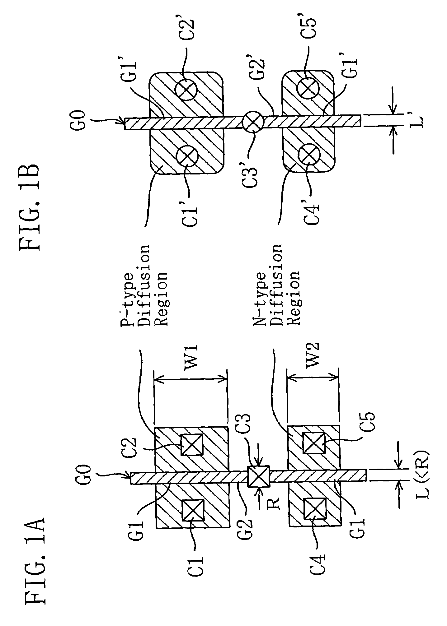
[0027]A first embodiment of the present invention will be described below with reference to the drawings. FIGS. 1A and 1B are a plan view of the design geometry of a semiconductor device (e.g., standard cell) according to the first embodiment of the invention, and a plan view of the geometry thereof after fabricated, respectively.

[0028]As shown in FIG. 1A, in the semiconductor device of the first embodiment, a gate polysilicon film is provided across a P-type diffusion region and an N-type diffusion region which are surrounded with an element isolation region made of STI or the like. Of the gate polysilicon film G0 which is used as a gate conductor film provided across the P-type and N-type diffusion regions and the element isolation region, its parts located on the P-type and N-type diffusion regions serve as gate electrode parts (gates) G1, and its part located on the element isolation region serves as a gate interconnect part G2. The gate interconnect part G2 is provided with a c...

second embodiment

[0033]The above first embodiment has described the structure of the semiconductor device which suppresses variations in the gate length of the MIS transistor due to the optical proximity effect by making the gate electrode linear (rectangular) and the dimension thereof in the gate length direction constant.

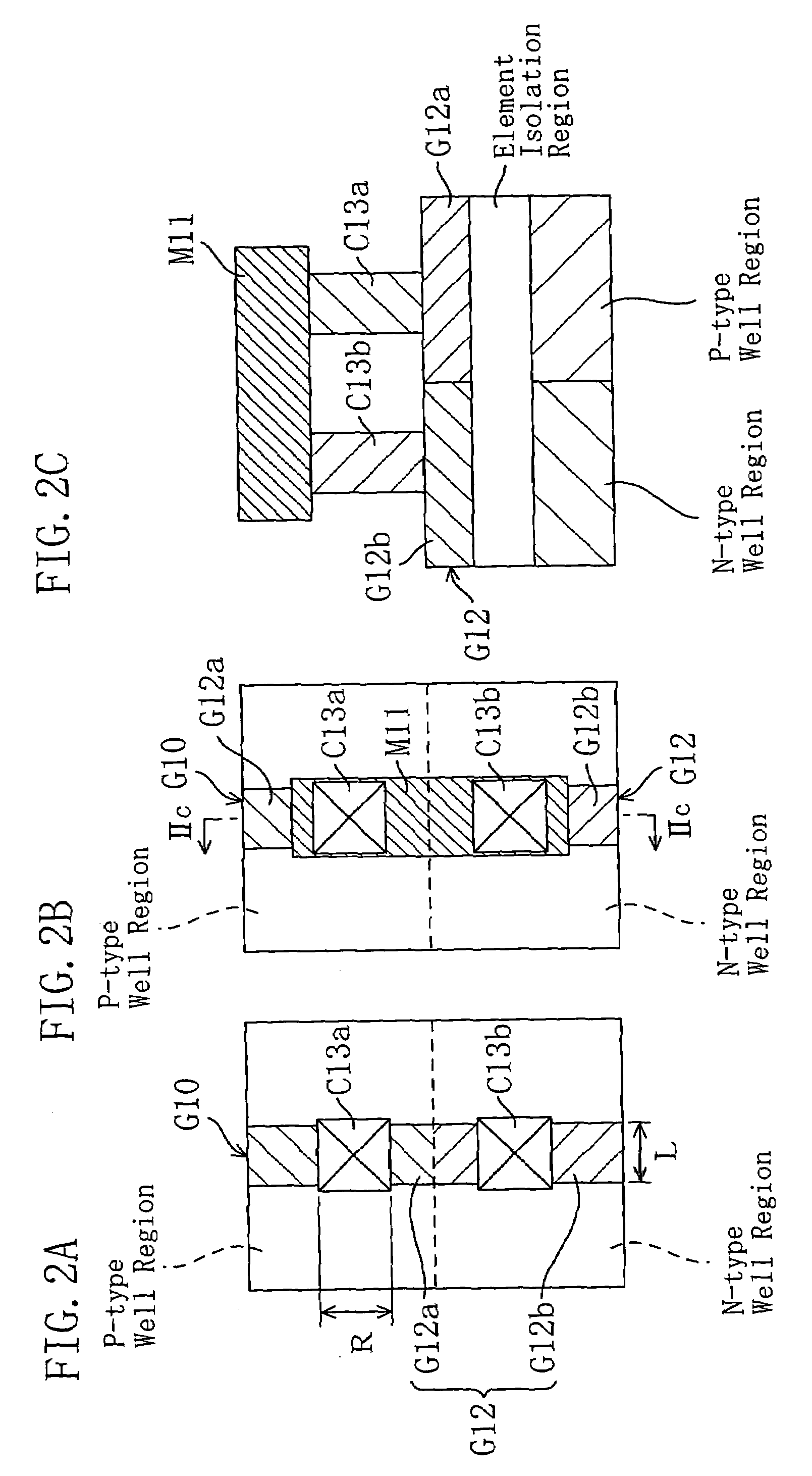
[0034]Now, in a CMOS device having a dual-gate structure, a p-type impurity is doped into the gate electrode of a P-channel MIS transistor, and an n-type impurity is doped into a gate electrode of an N-channel MIS transistor. Therefore, a gate polysilicon film includes part that provides an N-type polysilicon film on a P-type well region and part that provides a P-type polysilicon film on an N-type well region. Therefore, when the dimension of the gate polysilicon film in the gate length direction at the boundary between the N-type and the P-type polysilicon films is smaller than a certain value, the gate polysilicon film may be broken.

[0035]A second embodiment of the invention wi...

third embodiment

Modifications of Third Embodiment

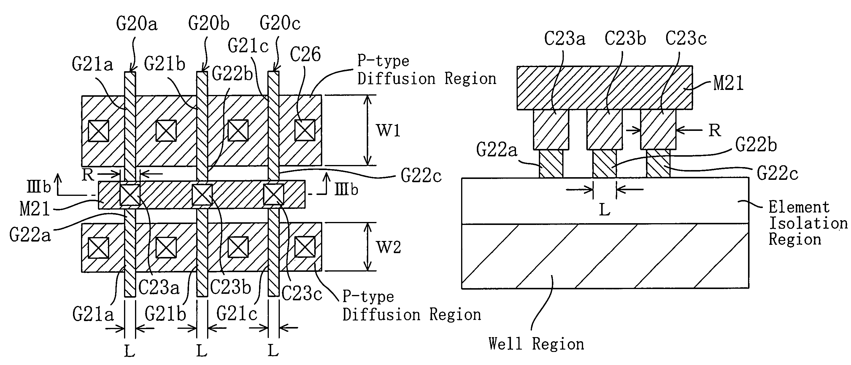
[0047]FIGS. 4A and 4B are a plan view illustrating a first modification of the third embodiment, and a cross sectional view illustrating a second modification thereof, respectively.

[0048]As shown in FIG. 4A, a semiconductor device according to the first modification of the third embodiment has, instead of the contacts provided on the gate interconnect parts and on part of the element isolation region located between the P-type and the. N-type diffusion regions, pairs of contacts C23a, C23a to C23c, C23c provided on the gate interconnect parts G22a to G22c and on parts of the element isolation region between which the P-type diffusion region and the N-type diffusion region are interposed. The semiconductor device also has a metal interconnect M21 provided on the pairs of contacts C23a, C23a to C23c, C23c to electrically connect the contacts C23a, C23a to C23c, C23c to one another. The structures of the gate polysilicon films G20a to G20c, the P-type ...


PUM


Abstract

A semiconductor device includes a semiconductor substrate; a diffusion region which is formed in the semiconductor substrate and serves as a region for the formation of a MIS transistor; an element isolation region surrounding the diffusion region; at least one gate conductor film which is formed across the diffusion region and the element isolation region, includes a gate electrode part located on the diffusion region and a gate interconnect part located on the element isolation region, and has a constant dimension in the gate length direction; and an interlayer insulating film covering the gate electrode. The semiconductor device further includes a gate contact which passes through the interlayer insulating film, is connected to the gate interconnect part, and has the dimension in the gate length direction larger than the gate interconnect part.

Description

CROSS-REFERENCE TO RELATED APPLICATIONS[0001]The present application claims priority under 35 USC 119(a) to Japanese Patent Application No. 2004-213903 filed on Jul. 22, 2004 the entire contents of which are hereby incorporated by reference.BACKGROUND OF THE INVENTION[0002](a) Field of the Invention[0003]The present invention relates to a semiconductor device having a miniaturized transistor, and particularly to a measure against an optical proximity effect.[0004](b) Description of the Related Art[0005]Main factors causing variations in propagation delay time in a design of a semiconductor integrated circuit (LSI) include variations in operating power supply voltage, temperature, process, etc. The LSI should be designed so that its operation is ensured even when all the factors are worst. Among determinants of a transistor, the gate length is a particularly important determinant which defines the operation of the transistor. The variations in the gate length thus affect variations i...

Claims


Application Information

Patent Timeline
Patent Type & Authority Patents(United States)
IPC IPC(8): H01L27/10
CPCH01L21/76895H01L27/0207H01L21/823475
Inventor IKOMA, DAISAKUKAJIYA, ATSUHIROOOTANI, KATSUHIROYAMASHITA, KYOJI
Owner GK BRIDGE 1
Why Eureka
Try Eureka