Electronic device manufacture

a technology of electronic devices and manufacturing methods, applied in the direction of photomechanical devices, high-frequency circuit adaptations, instruments, etc., can solve the problems of difficult deposition of metal layers, rough edges of apertures etched into porous dielectric materials, and problems such as the presence of such pores

Inactive Publication Date: 2007-11-13
SHIPLEY CO LLC
View PDF38 Cites 10 Cited by
  • Summary
  • Abstract
  • Description
  • Claims
  • Application Information

AI Technical Summary

Benefits of technology

[0057]The present invention provides several advantages in the manufacture of electronic devices: line edge or aperture sidewall roughness is reduced or eliminated, improved barrier layer performance is achieved due to the barrier layer being deposited on a smoother aperture sidewall surface, improved electrical conductivity of the copper aperture fill and reduced overall processing steps and time.

Problems solved by technology

However, in certain circumstances, the presence of such pores are problematic.
For example, apertures etched into such porous dielectric materials suffer from sidewall roughness due to the pores or voids in the dielectric material.
Such sidewall roughness creates difficulties in the subsequent deposition of metal layers such as barrier or seed layers.
Thus, roughness in the aperture sidewalls tends to create discontinuities in the barrier and / or seed layers.
These discontinuities can adversely affect subsequent processing steps in the manufacture of and the performance of electronic devices.

Method used


Image

  • Electronic device manufacture
  • Electronic device manufacture

Examples


Embodiment Construction

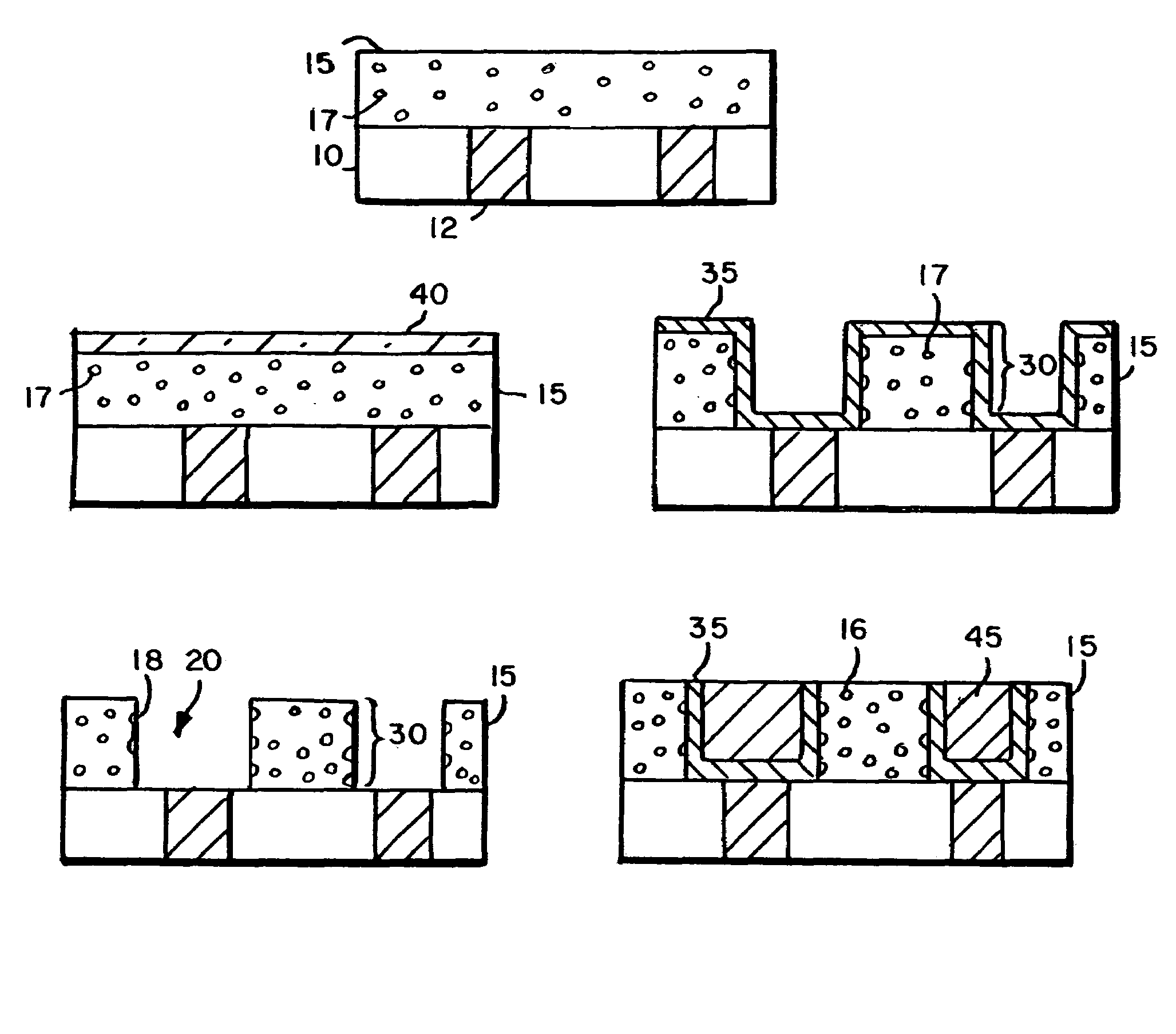
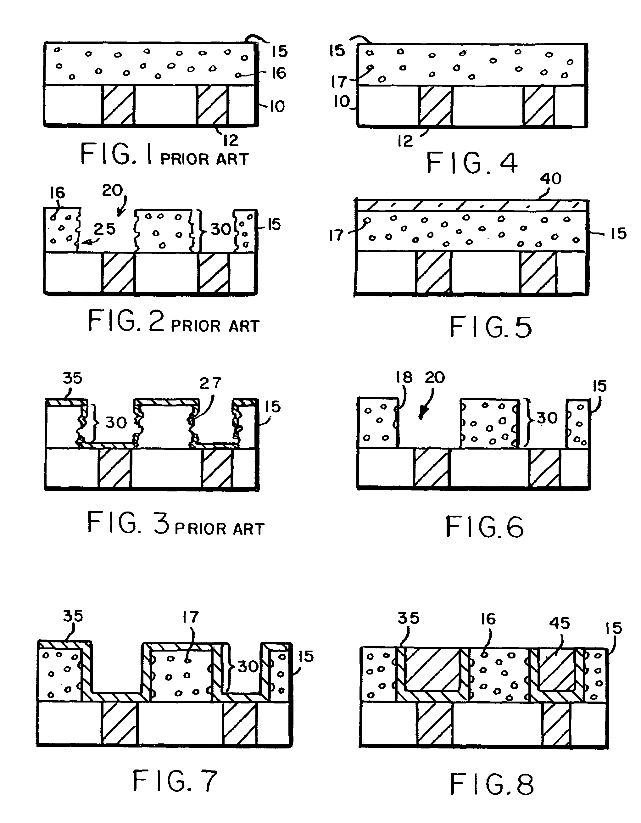
[0021]As used throughout this specification, the following abbreviations shall have the following meanings, unless the context clearly indicates otherwise: ° C.=degrees centigrade; UV=ultraviolet; and nm=nanometer. “Apertures” refer to any recessed features, such as for example, vias and trenches.

[0022]The term “alkyl” includes straight chain, branched and cyclic alkyl groups. The term “porogen” refers to a pore forming material or moiety, such as, but not limited to a compound that can be co-polymerized with the dielectric material to form a block co-polymer or a polymeric material or particle dispersed in a dielectric material, that is subsequently removed to yield pores, voids or free volume in the dielectric material. Thus, the terms “removable porogen,”“removable polymer” and “removable particle” are used interchangeably throughout this specification. The terms “pore,”“void” and “free volume” are used interchangeably throughout this specification. “Cross-linker” and “cross-link...


PUM

PropertyMeasurementUnit
mole ratiosaaaaaaaaaa
dielectric constantaaaaaaaaaa

Abstract

Disclosed are methods of manufacturing electronic devices, particularly integrated circuits. Such methods include the use of low dielectric constant material prepared by using a removable porogen material.

Description

[0001]This application is a continuation of U.S. patent application Ser. No. 10 / 394,342, filed on Mar. 22, 2003 now U.S. Pat. No. 7,163,780, which is a continuation of U.S. patent application Ser. No. 09 / 948,388, filed on Sep. 8, 2001, now U.S. Pat. No. 6,596,467, issued on Jul. 22, 2003 which claims the benefit of U.S. Provisional Application No. 60 / 232,127, filed on Sep. 13, 2000.BACKGROUND OF THE INVENTION[0002]The present invention relates generally to the field of manufacture of electronic devices. In particular, the present invention relates to the manufacture of integrated circuits containing low dielectric constant material.[0003]As electronic devices become smaller, there is a continuing desire in the electronics industry to increase the circuit density in electronic components, e.g., integrated circuits, circuit boards, multichip modules, chip test devices, and the like without degrading electrical performance, e.g., crosstalk or capacitive coupling, and also to increase t...

Claims


Application Information

Patent Timeline
Patent Type & Authority Patents(United States)
IPC IPC(8): G03F7/00B29C67/20H01L21/312H01L21/316H01L21/48H01L21/768H05K1/02
CPCB29C67/202H01L21/02137H01L21/02203H01L21/02282H01L21/3122H01L21/76802H01L21/7682H01L21/7684H05K1/024H01L21/481H01L21/31695Y10T428/24331H05K2201/0116H01L2221/1047H01L21/31
Inventor GALLAGHER, MICHAEL K.YOU, YUJIAN
Owner SHIPLEY CO LLC
Why Eureka
Try Eureka