Micro-engineered electron multipliers

a technology of electron multipliers and micro-engineers, applied in the direction of multiplier electrode arrangements, electric multiplier tubes, instruments, etc., can solve the problems of limited range of possible features, high processing cost, and restricted choice of coatings for secondary electron emission, so as to increase the effective resistance of semi-conducting links

Active Publication Date: 2007-11-13
MICROSAIC SYST
View PDF8 Cites 46 Cited by
  • Summary
  • Abstract
  • Description
  • Claims
  • Application Information

AI Technical Summary

Benefits of technology

[0015]This invention provides for a simple method of fabricating miniature electron multipliers in an in-plane configuration for use with miniature analytic instruments such as mass filters. The materials involved are predominantly silicon and compatible oxides, thereby allowing the possibility of integration with a mass filter formed in a similar materials system. The materials are selected simultaneously to withstand high voltages and to enhance secondary electron emission. The fabrication system and methodology of the present invention also allows the construction of an integrated set of bias resistors in a device containing multiple electrodes, so that the device may be operated from a single high-voltage source. These features overcome many of the drawbacks in the prior art described above.
[0027]Preferably, each of the elements forming a Venetian blind structure is formed at an angle offset from the intended path of incoming electrons thereby increasing the probability of interaction with incoming electrons.
[0031]Such oxidised surfaces or coatings may be doped with an additional material to enhance secondary electron emission. The oxide surface may also be annealed in hydrogen or some other reducing agent to enhance secondary electron emission.
[0033]Certain embodiments may electrically couple adjacent electrodes to one another by a series of semi-conducting links. The semi-conducting links may be connected to act as bias resistors. Oxidation may be used to increase the effective resistance of the semiconducting links. It will be appreciated that the bias resistors may form a set of resistors linking and biasing a dynode chain.
[0040]d) Annealing the oxidised silicon structure so as to provide enhanced secondary electron emission functionality,

Problems solved by technology

Features with arbitrary shapes may be formed, in an orientation normal to the substrate plane; however, the process is expensive, and the features are formed in non-silicon materials such as electroplated metal.
Although these materials can be modified with additional surface coatings, the choice of coatings that may be used for secondary electron emission is restricted.
However, the range of possible features is limited, because the process forms structures that are bounded by specific crystal planes (typically, the plane).
As a result, it is not possible to form arbitrary features orientated normal to the substrate plane.
However, it is unclear whether the device was actually fabricated, and issues relating to suitable materials do not seem to have been addressed.
2000); however, very little attention has been paid to the equally important problem of detector miniaturisation and integration.
However, to date no such structures are available.
However, the electron multiplier devices described above are generally not compatible with such a scheme.
Connection to the individual electrodes is also complex, requiring many separate electrical wires.

Method used


Image

  • Micro-engineered electron multipliers
  • Micro-engineered electron multipliers
  • Micro-engineered electron multipliers

Examples


Embodiment Construction

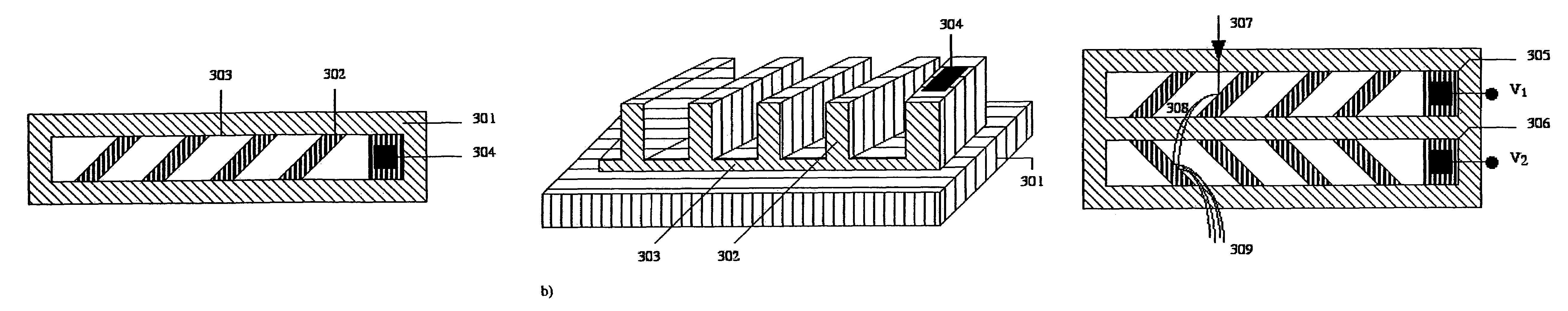
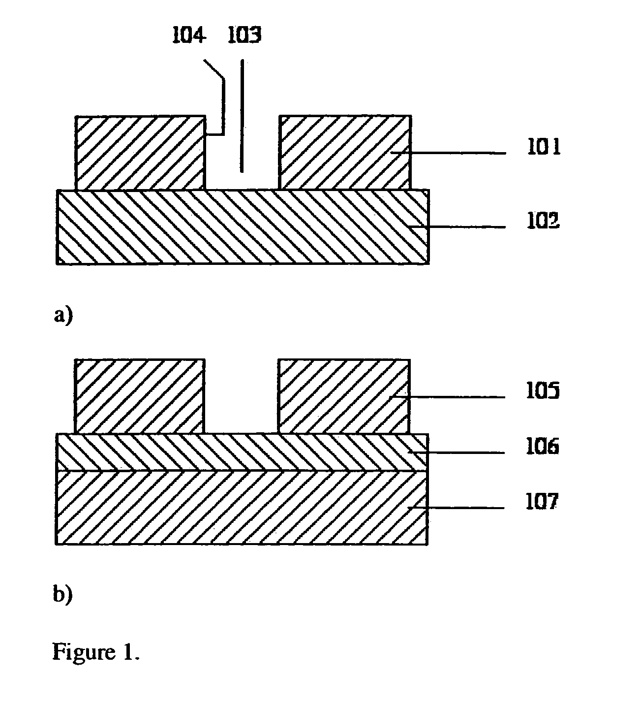
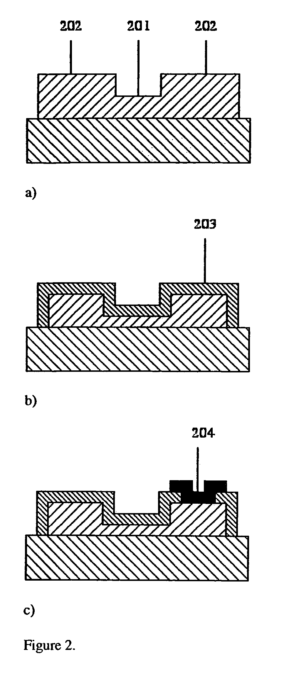
[0055]A detailed description of the invention is now provided, with reference to FIGS. 1-5.

[0056]FIG. 1a shows a cross-section of a silicon-on-glass wafer, which consists of a first material provided by a silicon layer 101 bonded to a second material provided by a glass or silica layer 102. The first material is a semiconductor, which may be converted into an insulator with enhanced secondary emission properties by oxidation and subsequent annealing at high temperature in hydrogen gas. It will be appreciated that in this context, the hydrogen is acting as a reducing agent and that other reducing agents could equivalently be used for specific applications. The second layer provides an insulating substrate. Using a single layer of patterning, the silicon layer 101 may be structured by deep reactive ion etching (DRIE) to form vertical features 103, stopping at the interface between the two materials. It will be appreciated that each vertical feature forms a structure with sidewalls 104...


PUM


Abstract

This invention provides for a simple method of fabricating miniature electron multipliers, in an in-plane configuration suitable for use with miniature analytic instruments such as mass filters. The materials involved are predominantly silicon and compatible oxides, allowing the possibility of integration with a mass filter formed in a similar materials system. The materials are selected simultaneously to withstand high voltages and to enhance secondary electron emission. Fabrication is based on standard planar processing methods. These methods also allow the construction of an integrated set of bias resistors in a multi-electrode device, so that the device may be operated from a single high-voltage source.

Description

[0001]This application claims priority from British Application No. GB0400399.2, filed 9 Jan. 2004 (incorporated by reference herein).FIELD OF THE INVENTION[0002]The invention relates to electron multipliers and particularly to electron multipliers formed in a Microelectromechanical system (MEMS) environment.BACKGROUND[0003]Originally developed for early TV cameras, electron multipliers are of considerable importance in low-signal light detection, night vision and mass spectrometry, and in instrumentation for high-energy physics. They provide an analogous function to the erbium doped fibre amplifier in optical communications, namely low-noise, high gain pre-detector amplification. There are a wide variety of different configurations, including discrete dynode devices and mesh multipliers, and continuous dynode devices such as microchannel plates and channeltron multipliers. Variants such as the Gas Electron Multiplier (GEM) are used for particle detection. Some types (e.g. microchan...

Claims


Application Information

Patent Timeline
Patent Type & Authority Patents(United States)
IPC IPC(8): H01J40/00H01J9/12H01J40/14H01J43/22
CPCH01J9/125H01J43/246H01J43/22
Inventor SYMS, RICHARD
Owner MICROSAIC SYST
Why Eureka
Try Eureka