Sputtering target, sintered compact, electrically conductive film produced by using the same, and organic EL device and substrate used for the same

a technology of electrically conductive film and sintered compact, which is applied in the direction of solid-state devices, conductive layers on insulating supports, natural mineral layered products, etc., can solve problems such as leakage current, and achieve the effect of reducing the efficiency of hole injection and high resistan

Inactive Publication Date: 2007-12-11
IDEMITSU KOSAN CO LTD
View PDF10 Cites 40 Cited by
  • Summary
  • Abstract
  • Description
  • Claims
  • Application Information

AI Technical Summary

Benefits of technology

[0231]The present invention is the invention set forth in 1 above, the configuration of which is changed in order. That is, the order of lamination of the transparent conductive thin film containing indium oxide and the metal thin wire is inverted. Even in such a configuration, the functions and effects of the invention are the same as in 1 above.
[0232]3. The present invention is characterized in that the thin film layer of the metal oxide has a specific resistance with the range of 10E+04 Ωcm and 10E+08 Ωcm.
[0233]The reason is that if the specific resistance is 10E+4 Ωcm or lower, the inter-anode resistance decreases to cause crosstalk. Moreover, if the specific resistance is 10E+8 Ωcm or higher, the resistance becomes so high that the hole injection efficiency may drop.
[0234]4. The present invention is characterized in that a thin film layer of the metal oxide layer has a work function of 5.8 eV or higher.
[0235]As described above, the work function is preferably 5.8 eV or higher, and yet preferably 6.0 eV or higher.
[0236]5. The present invention is characterized in that the metal oxide contains at least either one of zinc oxide and tin oxide.

Problems solved by technology

Nevertheless, there has been a known problem that organic luminescent layers, being organic materials, are typically difficult to transport electrons and holes through and thus prone to deterioration, easily causing a leak current due to secular changes over a long time of use.

Method used


Image

  • Sputtering target, sintered compact, electrically conductive film produced by using the same, and organic EL device and substrate used for the same
  • Sputtering target, sintered compact, electrically conductive film produced by using the same, and organic EL device and substrate used for the same
  • Sputtering target, sintered compact, electrically conductive film produced by using the same, and organic EL device and substrate used for the same

Examples


embodiments 1

GROUP OF EMBODIMENTS 1

[0274]Hereinafter, a group of embodiments 1 of the present invention will be described with reference to the drawings.

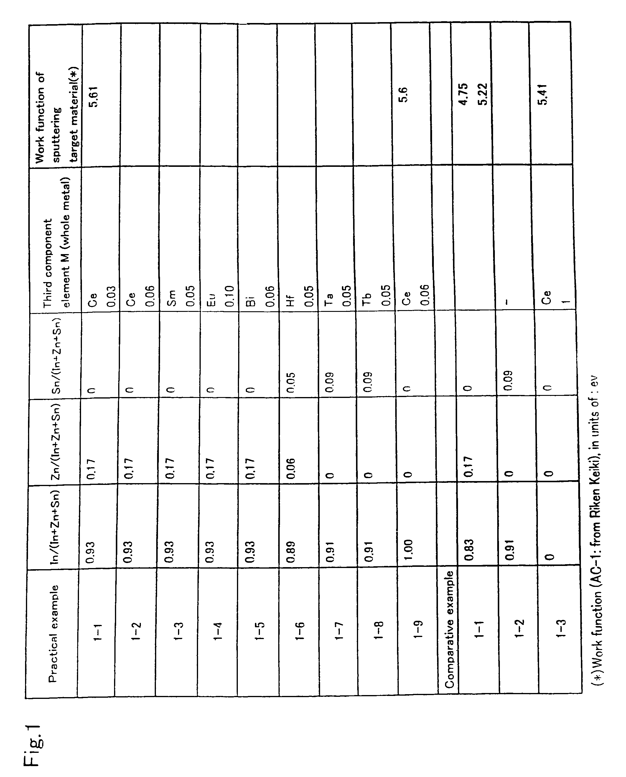
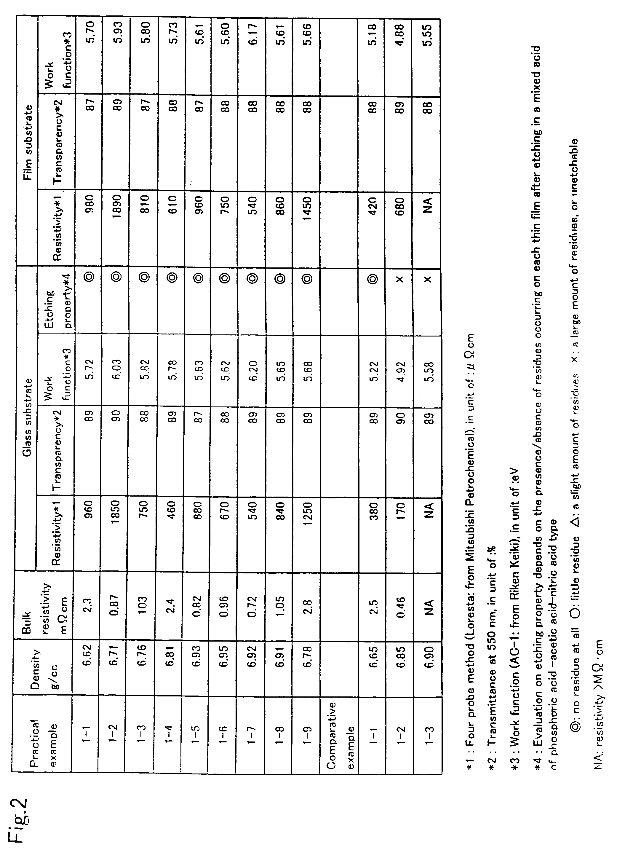
[0275]In the present embodiment, indium oxide, zinc oxide, and tin oxide powders were mixed in predetermined proportions. In addition, a predetermined amount of cerium oxide, samarium oxide, europium oxide, terbium oxide, or bismuth oxide powder was measured and mixed therein as a third component. This mixture was ground in a wet grinder for 48 hours, and then dry granulated and press molded before it was sintered at 1380-1480° C. into a sintered article. This sintered article corresponds to an example of the sputtering target in claims.

[0276]Moreover, when the mixture is of indium oxide and zinc oxide, it contain a hexagonal layered compound comprising indium oxide and zinc oxide (In2O3(ZnO)m: where m is an integer of 2 to 20). For instance, in practical examples 1-1 to 1-6 to be described later, the inclusion of such a hexagonal layered compou...

embodiments 2

GROUP OF EMBODIMENTS 2

Embodiment 2-1

[0310]Initially, with reference to FIG. 3, description will be given of an embodiment 2-1 according to the organic EL device of the present invention. FIG. 3 is a sectional view of an organic EL device 100. As shown in this diagram, the organic EL device 100 has the structure that an anode layer 10, an organic luminescent layer 14, and a cathode layer 16 are laminated on a substrate (not shown) in succession.

[0311]Hereinafter, description will concentrate on the anode layer 10 and the organic luminescent layer 14 which are the characteristic parts of the embodiment 2-1. The configuration and forming method of the rest of the components, such as the cathode layer 16, will be described in the briefest form. As for parts that are not mentioned, various configurations and forming methods generally known in the field of organic EL devices may be employed.

[0312]Incidentally, in the embodiment 2-1, the anode layer 10 is made of compounds of group A-1 or ...

embodiment 2-2

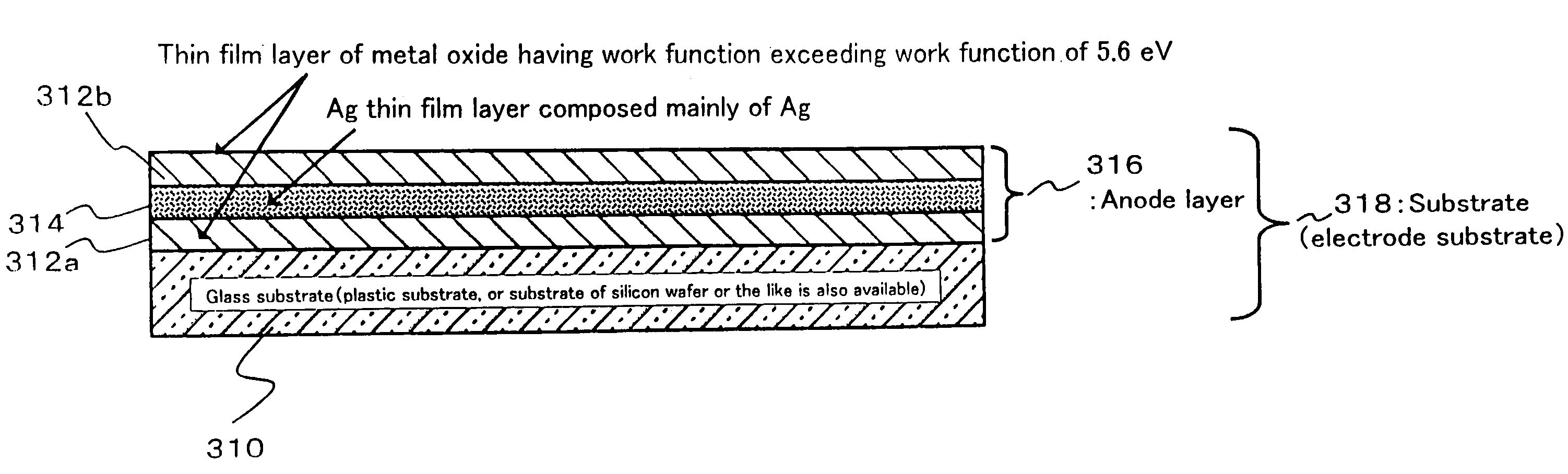
[0366]Next, with reference to FIG. 4, description will be given of an embodiment 2-2 of this invention. FIG. 4 is a sectional view of an organic EL device 102 according to the embodiment 2-2, showing the device having the structure that an anode layer 10, an inorganic thin film layer 12, an organic luminescent layer 14, and a cathode layer 16 are laminated on a substrate (not shown) in succession. When the inorganic thin film layer 12 is provided thus, injected holes can be transported effectively. Consequently, the provision of the inorganic thin film layer 12 allows low-voltage driving and improves the durability of the organic EL device 102.

[0367]Incidentally, the organic EL device 102 of the embodiment 2-2 is characterized in that the inorganic thin film layer 12 is interposed between the anode layer 10 and the organic luminescent layer 14. In other respects, it has the same structure as that of the organic EL device 100 of the embodiment 2-1.

[0368]Hence, the following descripti...


PUM

PropertyMeasurementUnit
work functionaaaaaaaaaa
transmittanceaaaaaaaaaa

Abstract

A sintered article is fabricated which contains one or more of indium oxide, zinc oxide, and tin oxide as a component thereof and contains any one or more types of metal out of hafnium oxide, tantalum oxide, lanthanide oxide, and bismuth oxide. A backing plate is attached to this sintered article to constitute a sputtering target. This sputtering target is used to fabricate a conductive film on a predetermined substrate by sputtering. This conductive film achieves a large work function while maintaining as much transparency as heretofore. This conductive film can be used to achieve an EL device or the like of improved hole injection efficiency.

Description

TECHNICAL FIELD[0001]The present invention relates to a transparent conductive film for use in an LCD (Liquid Crystal Display), an organic EL (Electroluminescence) device, and the like, and more particularly to the material thereof. The invention also relates to a sintered article and a sputtering target having the same composition as that of the material. Besides, the invention relates to a sputtering target which is made of this sintered article or the like and is intended for the formation of the transparent conductive film.[0002]Moreover, the invention relates to the foregoing organic EL (electroluminescence) device, a substrate for use in this organic EL device, and a method of fabricating the same. To be more specific, the invention relates to an organic EL device which is suitably applicable to displays, the light sources of printer heads, and the like in consumer and industrial applications, a substrate for use in the organic EL device, and a method of fabricating the same.[...

Claims


Application Information

Patent Timeline
Patent Type & Authority Patents(United States)
IPC IPC(8): B32B9/00C04B35/00C04B35/50C23C14/08C23C14/34H01B5/14H01L51/00H01L51/40H01L51/50H01L51/52
CPCC04B35/01C04B35/50C23C14/086C23C14/3414H01L51/5206H01L51/5221C04B35/453Y10T428/12618C04B2235/3224C04B2235/3229C04B2235/3244C04B2235/3251C04B2235/3284C04B2235/3286C04B2235/3287C04B2235/3293C04B2235/3294C04B2235/3298C04B2235/77C04B2235/96C04B2235/9653H01L51/0021H01L51/5012H01L51/5048H01L51/5088H01L51/5092H10K71/60H10K50/11H10K50/14H10K50/17H10K50/171H10K50/81H10K50/816H10K50/82C23C14/34H05B33/10C09K11/06
Inventor INOUE, KAZUYOSHIKAWAMURA, HISAYUKI
Owner IDEMITSU KOSAN CO LTD
Why Eureka
Try Eureka