Semiconductor device to improve data retention characteristics of DRAM

a technology of dram and semiconductors, applied in the field of semiconductor devices, can solve the problems of inability to prevent the defective cell caused by these factors, the difficulty of substantial improvement of the retention cycle, and the increase of the area due to that becoming a disadvantage, so as to improve the data retention characteristic, reduce power consumption, and improve the effect of data retention characteristics

Inactive Publication Date: 2008-01-01
SONY CORP
View PDF6 Cites 18 Cited by
  • Summary
  • Abstract
  • Description
  • Claims
  • Application Information

AI Technical Summary

Benefits of technology

[0017]The present invention is to provide a semiconductor device able to improve data retaining characteristics, decrease power consumption, and further able to realize a more unrestricted system without increasing excessive circuits.

Problems solved by technology

Moreover, a defective cell caused by these factors cannot be prevented even if an improvement of the producing processing is performed.
However, the method has to add the redundancy cell in accordance with the number of defect to be secured, and the increase of area due to that becomes a disadvantage.
Further, since the number of the redundancy cells to be mountable is restricted, a substantial improvement of the retention cycle is difficult.
When designing a circuit able to generate efficient patterns, the circuit size becomes large, and when making the circuit size small, a pattern becomes redundant and an operating time increases, so that it is caught in a dilemma.
Then, as usual, only the minimum necessary circuits are mounted, but the pattern becomes redundant as mentioned above, and the operation time becomes a disadvantage.
Due to the above mentioned factors, the semiconductor integrated circuit system in the above document has the following disadvantages: (1) to mount the exclusive circuit causes an increase in excessive circuits; and (2) keeping the circuit size small, causes an increase in operating time.

Method used


Image

  • Semiconductor device to improve data retention characteristics of DRAM
  • Semiconductor device to improve data retention characteristics of DRAM
  • Semiconductor device to improve data retention characteristics of DRAM

Examples


Embodiment Construction

[0057]Next, preferred embodiments of the present invention will be explained with reference to the drawings.

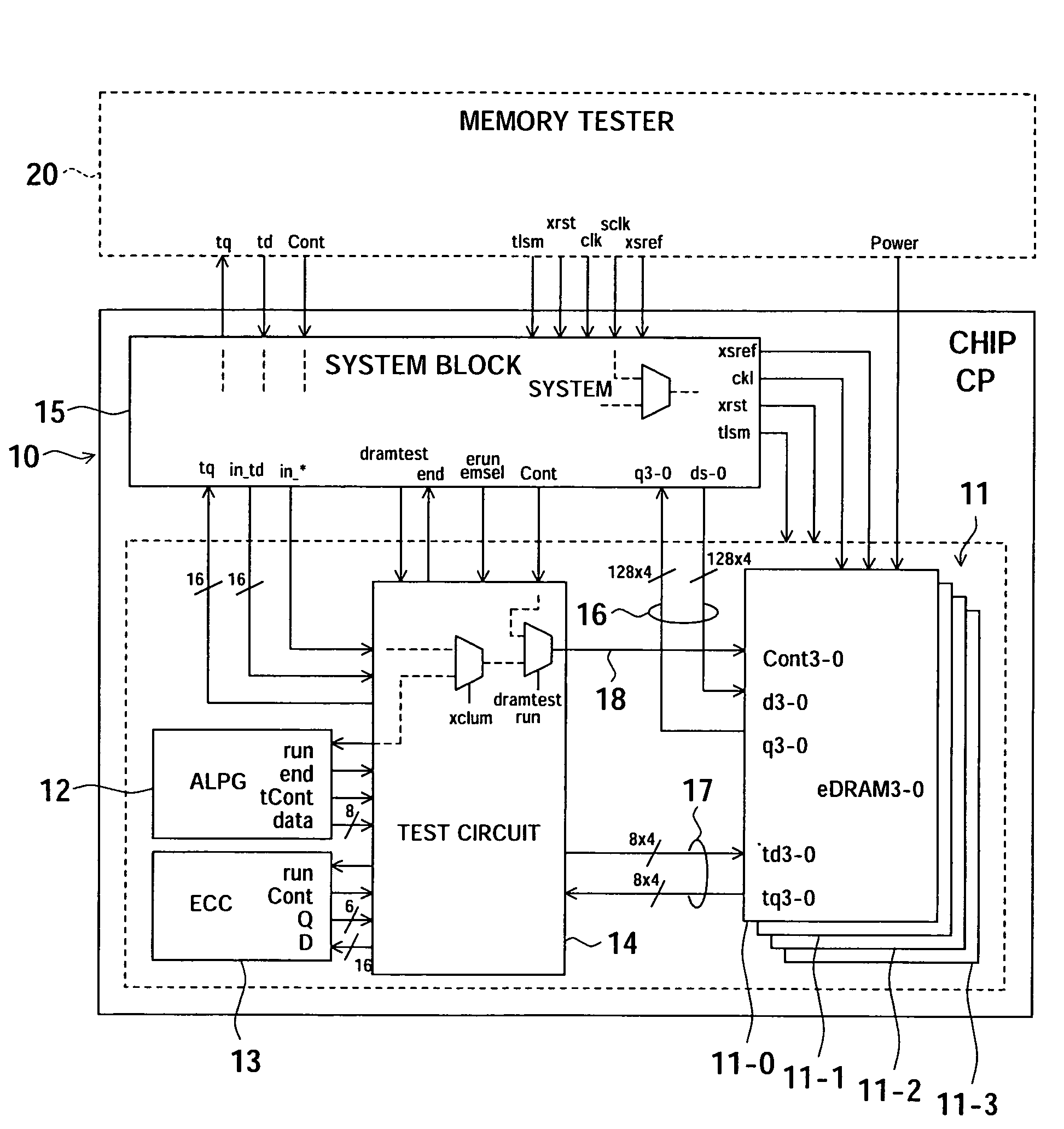
[0058]FIG. 1 is a system configuration view showing an embodiment of a semiconductor device of an embodiment.

[0059]A semiconductor device 10 according to the present embodiment has a DRAM circuit 11, an algorithmic pattern generator (ALPG) 12 as a DRAM pattern generating circuit, an ECC circuit 13 as an error correcting circuit, a test circuit 14 as an interface circuit, and a system block 15, and the semiconductor device is formed by integrating them on a single chip CP.

[0060]The semiconductor device 10 according to the present embodiment connects a memory tester 20 outside of the chip CP to the system block 15 and can perform the predetermined test with respect to the DRAM circuit (eDRAM 0 to 3) 11.

[0061]The semiconductor device 10 generates a parity bit when introducing a standby state and corrects DRAM data by the ECC circuit (an ECC decoder) when returning from the standb...


PUM


Abstract

A semiconductor device able to improve data retaining characteristics and decrease power consumption, further able to realize more unrestricted system without increasing excessive circuits, and having the following: an ALPG receiving a start signal and a mode selection signal to generate commands and addresses with respect to a DRAM circuit with the predetermined patterns in accordance with modes, and outputting an ending signal when ending a pattern generating processing in each of modes; an ECC circuit receiving a start signal and a mode selection signal indicating a parity generation mode to generate a parity based on data read from the DRAM circuit, receiving the start signal and a mode selection signal indicating an error correction mode to perform an error correction with respect to data read from the DRAM circuit based on the parity generated in the parity generation mode and outputting data after correcting; and an interface circuit.

Description

CROSS REFERENCES TO RERATED APPLICATIONS[0001]The present invention contains subject matter related to Japanese Patent Application JP 2004-081505 filed in the Japanese Patent Office on Mar. 19, 2004 and Japanese Patent Application JP 2004-173853 filed in the Japanese Patent Office on Jun. 11, 2004, the entire contents of which are incorporated herein by reference.BACKGROUND OF THE INVENTION[0002]1. Field of the Invention[0003]The present invention relates to a semiconductor device embedding a dynamic random access memory (DRAM), in particular, a system circuit for improving data retaining characteristics of the DRAM.[0004]2. Description of the Related Art[0005]In general, data retaining characteristics of DRAMs has been decided, for example, by the poorest one of the memory cells to be mounted.[0006]The characteristics of DRAMs have been decided by a leakage current characteristic caused by a crystal defect in the memory cell and observed as a random defect of a single bit at a memo...

Claims


Application Information

Patent Timeline
Patent Type & Authority Patents(United States)
IPC IPC(8): G01R31/28G06F11/00G06F12/00G06F13/00G06F13/28G11C29/00H03M13/00H01L27/108G06F13/16G11C11/401G11C11/406G11C29/12G11C29/42H01L21/8242
CPCG06F11/106G06F13/1689Y02B60/1228Y02D10/00
Inventor ARAKAWA, TOMOFUMIKODAMA, HIROAKIINOUE, KAZUTOSHI
Owner SONY CORP
Why Eureka
Try Eureka