Method of producing polymer optical waveguide

a technology of optical waveguides and polymers, applied in the field of producing polymer optical waveguides, can solve the problems of affecting the accuracy of a core diameter, the application of films, and the cost of methods (2) and (3), and achieve the effects of preventing the mingling of air cells, reducing costs, and easy formation

Inactive Publication Date: 2008-01-08
FUJIFILM BUSINESS INNOVATION CORP
View PDF5 Cites 10 Cited by
  • Summary
  • Abstract
  • Description
  • Claims
  • Application Information

AI Technical Summary

Benefits of technology

[0021]The present invention has been made in view of the above-described circumstances and provides a method of producing at extremely low cost, by a much simplified method, a flexible polymer optical waveguide with a very modest loss in propagation.
[0025]The method of producing a polymer optical waveguide according to the invention involves a much simplified production process, enabling a polymer optical waveguide to be formed easily and makes it possible to manufacture a polymer optical waveguide at a substantially lower costs than conventional methods of producing an polymer optical waveguide. Moreover, since though-holes are formed in the mold to suck the core-forming curable resin exit side under reduced pressure, adhesion between the mold and the film base substrate is improved, and this can prevent the mingling of air cells. Further, since a lower clad layer with a flat surface is formed on the lower film and the core is formed on the lower clad layer, it has become possible to reduce propagation loss substantially (0.1 dB / cm or less).
[0026]Accordingly, the polymer optical waveguide produced according to the production method of the invention is a flexible polymer optical waveguide with a substantial reduction in propagation loss, and a high degree of accuracy. Moreover, the polymer optical waveguide can be freely packaged on various devices. In addition, the film base substrate can be selected freely in the invention, an expensive clad film can be avoided and an inexpensive film base substrate may be used, thus making it possible to manufacture at low costs a polymer optical waveguide which has a high degree of heat resistance, a lower level of propagation loss and a high degree of accuracy.

Problems solved by technology

However, in the selective polymerization method (1) a problem exists in the application of the film, methods (2) and (3) are expensive because a photolithographic method is entailed and in method (4) a problem exists surrounding the accuracy of a core diameter.
Furthermore, method (5) also entails a problem insofar that a sufficient difference cannot be obtained between the refractive indices of the core layer and the clad layer.
However, as mentioned above, both of these methods give rise to a problem of costs.
Moreover, not one of methods (1) to (5) is appropriate for forming a polymer optical waveguide on a flexible plastic base material covering large area.
However, when this method has been used, difficulties have occurred insofar that the polymer precursor material is introduced not only into the capillary groove but also spreads thinly over the entire space between the pattern substrate and the plane substrate.
In consequence, when the polymer precursor material applied between both substrates is cured, a thin layer having the same composition as the core layer is formed, resulting in the leaking of light through the thin layer.
However, since according to this method a monomer is used as the core-forming material, a problem arises insofar that when the monomer is polymerized into a polymer, the volume shrinkage factor is substantial and transmission loss of the polymer optical waveguide is magnified.
Moreover, this method is so complicated that the patterned substrate needs to be secured to the plane substrate by a clamp and in addition, the contact part has to be sealed with a resin.
This process is therefore unsuitable for mass-production, and in consequence no reduction in costs can be expected.
Also, it is impossible to apply this method to the production of a polymer optical waveguide using as the clad a film having a thickness of several mm or 1 mm or less.
However, even if the production method described in this patent were applied to the production of a polymer optical waveguide, because the core part of the optical waveguide has a small sectional area, considerable time would be required to form the core part, thus rendering the method unfit for mass-production.
There is also another drawback with this method insofar that a change in volume is caused when the monomer solution is polymerized to form a polymer, resulting in a change in the shape of the core and accordingly a substantial loss in transmission.
However, if an optical waveguide were manufactured according to the kind of micro-mold method mentioned above, it would be impossible to make the volume shrinkage factor smaller during curing (and thus reduce transmission loss), and at the same time reduce the viscosity of a filler liquid (monomer or the like) to make introduction easy.
Therefore, if priority is to be given to reducing transmission loss, it is not possible to maintain the viscosity of the filler liquid within a certain limit.
This results in a low speed of introduction and mass-production can not be expected.
Moreover, the aforementioned micro-mold method is based on the premise that a glass or silicon substrate will be used as the substrate and does not take into account the use of the kind of flexible film base material used in this method.
It is however difficult to introduce a core resin into only the concave portion and it is therefore difficult to manufacture a fine core pattern with a high degree of accuracy.
However, in the case of optical fibers, the end surfaces of the optical fiber must be abraded and optical connectors for connection purposes are also expensive.
However, if the film is thin, its handling is difficult and a semiconductor process, a highly accurate processing method, cannot be used.
However, this polymer optical waveguide still leaves further room for improvements in the reduction of propagation loss.

Method used


Image

  • Method of producing polymer optical waveguide
  • Method of producing polymer optical waveguide
  • Method of producing polymer optical waveguide

Examples


example 1

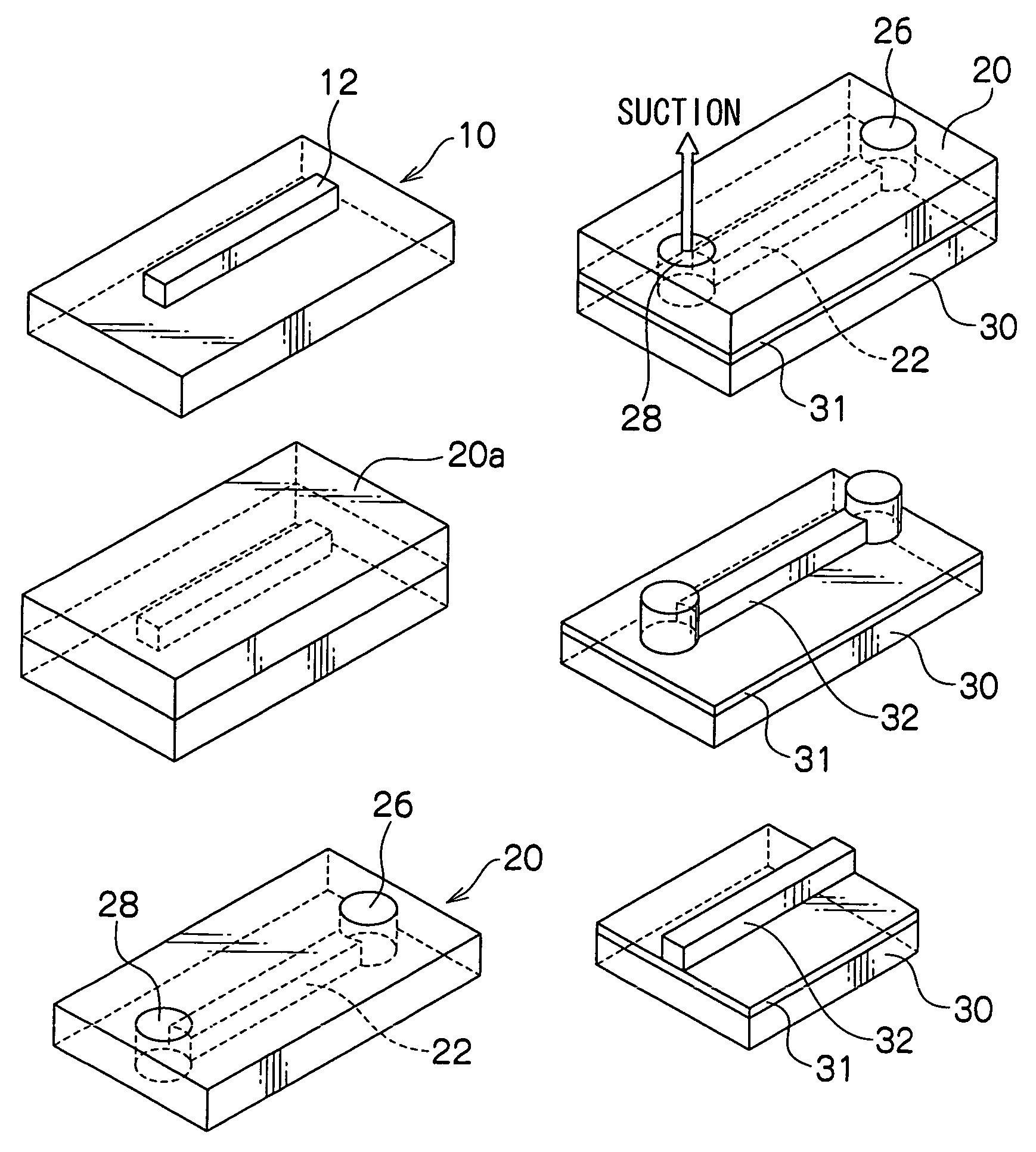
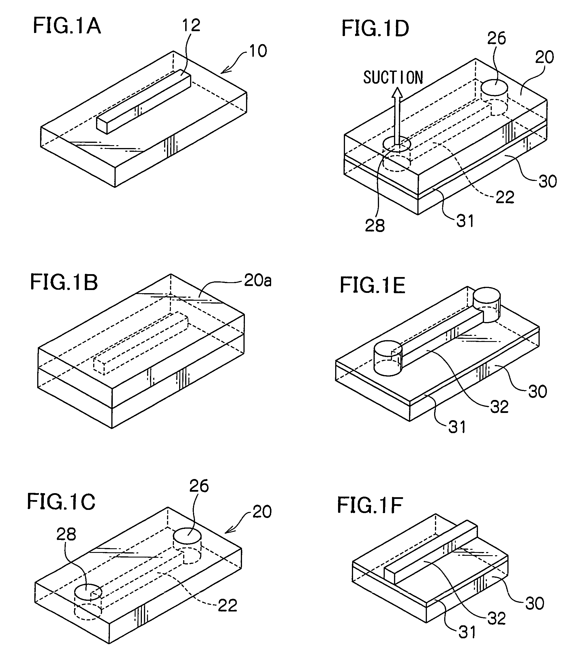
[0118]A thick film resist (SU-8, manufactured by MicroChem Corp.) is applied to a silicon (Si) substrate by a spin coating method, prebaked at 80° C., exposed to light through a photomask and developed to form 8 convex portions each having a square section (width: 50 μm, height: 50 μm and length: 80 mm). Intervals between the convex portions are designed to be 250 μm. Next, the substrate is post-baked at 120° C. to manufacture a master plate for manufacturing a polymer optical waveguide.

[0119]Next, a releasing agent is applied to the master plate, into which a mixture of a thermosetting liquid dimethylsiloxane rubber (SYLGARD 184, manufactured by Dow Coning Asia, viscosity: 5000 mPa·s) and a curing agent are introduced and heated at 120° C. for 30 minutes and then cured. The cured layer is then peeled off to manufacture a mold (thickness of the mold: 5 mm) having a concave portion and corresponding to the aforementioned rectangular convex portion.

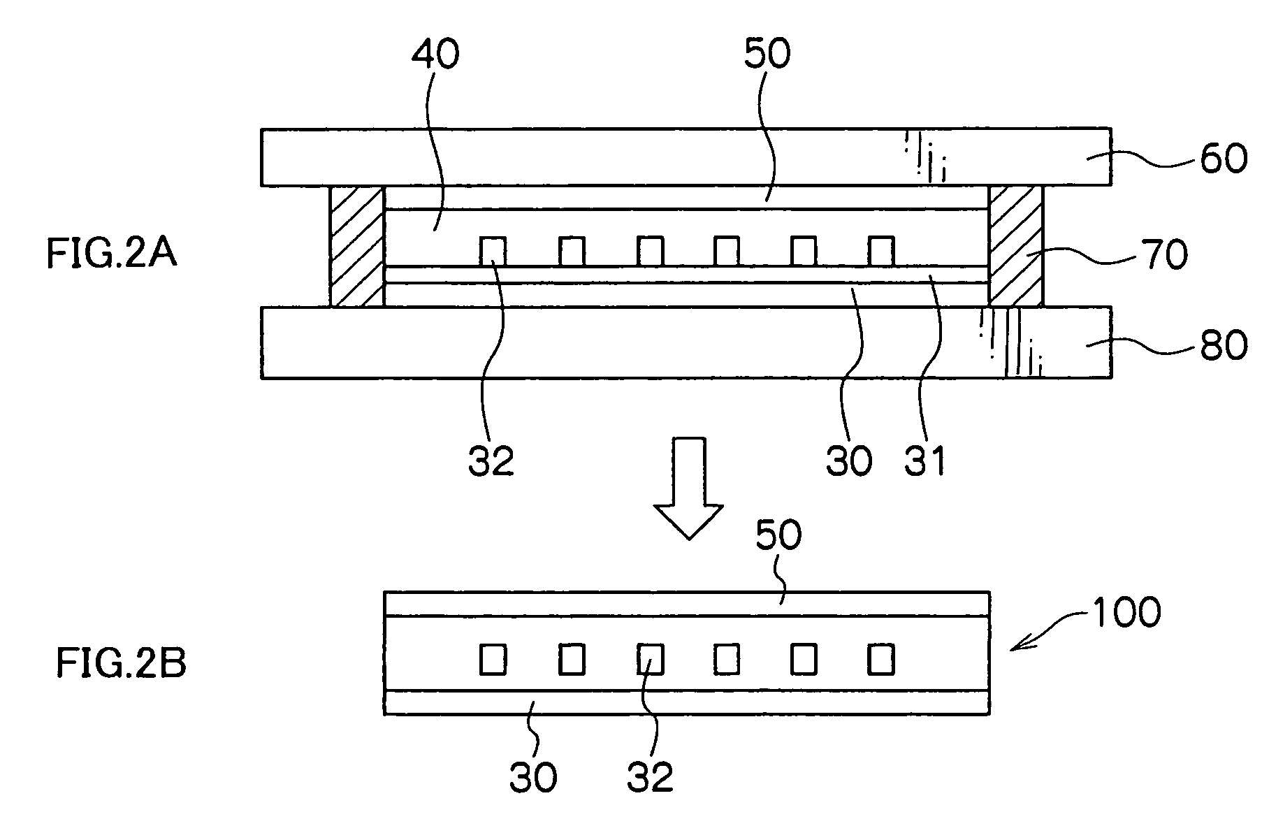
[0120]Moreover, through-holes each h...

example 2

[0128]A flexible polymer optical waveguide is manufactured in the same manner as in Example 1 except insofar that a polyether ether ketone (PEEK) film is used in place of the PES film.

[0129]The propagation loss of the polymer waveguide thus obtained is 0.06 dB / cm.

example 3

[0130]A flexible polymer optical waveguide is manufactured in the same manner as in Example 1 except insofar that an Arton film is used in place of the PES film.

[0131]The propagation loss of the polymer waveguide thus obtained is 0.06 dB / cm.


PUM

PropertyMeasurementUnit
thicknessaaaaaaaaaa
surface roughnessaaaaaaaaaa
curing shrinkage factoraaaaaaaaaa

Abstract

A method of producing a polymer optical waveguide, including: preparing a mold; preparing a lower film base material; introducing a core-forming curable resin into a first through-hole of the mold with which the lower film base material is brought into close contact while sucking the concave portion of the mold from a second through-hole under reduced pressure to introduce the core-forming curable resin into the concave portion of the mold; curing the core-forming curable resin which has been introduced; removing the mold from the lower film base material; providing a clad-forming curable resin layer and an upper film base material, the clad-forming curable resin layer being sandwiched between the lower film base material, on which the core is formed, and the upper film base material; and curing the clad-forming curable resin layer to fix the lower film base material and the upper film base material.

Description

CROSS-REFERENCE TO RELATED APPLICATION[0001]This application claims priority under 35USC 119 from Japanese Patent Application No. 2004-9428, the disclosure of which is incorporated by reference herein.BACKGROUND OF THE INVENTION[0002]1. Field of the Invention[0003]The present invention relates to a method of producing a polymer optical waveguide, and, particularly, to a polymer optical waveguide having a thin flexible filmy form.[0004]2. Description of the Related Art[0005]Among methods of producing a polymer waveguide, the following methods have been proposed: (1) a method in which a film is impregnated with a monomer, the core part is selectively exposed to light to change the refractive index and the film is then applied (a selective polymerization method), (2) a method in which a core layer and a clad layer are applied, and a clad part is then formed by using reactive ion etching (the RIE method), (3) a type of photolithographic method in which an ultraviolet ray-curable resin o...

Claims


Application Information

Patent Timeline
Patent Type & Authority Patents(United States)
IPC IPC(8): G02B6/10G02B6/00G02B6/13B29C33/38B29C39/24B29C39/42B29C43/14B29D11/00G02B6/12G02B6/138
CPCB29C39/24B29C39/42B29C43/146B29D11/00663G02B6/138B29C33/3842B29C33/3857B29C2043/148B29C2043/562G02B2006/12097B29C37/005B29C37/0067
Inventor OHTSU, SHIGEMISHIMIZU, KEISHIYATSUDA, KAZUTOSHIAKUTSU, EIICHI
Owner FUJIFILM BUSINESS INNOVATION CORP
Why Eureka
Try Eureka