Sequential lateral solidification device

Active Publication Date: 2008-02-05
LG DISPLAY CO LTD
View PDF41 Cites 67 Cited by
  • Summary
  • Abstract
  • Description
  • Claims
  • Application Information

AI Technical Summary

Benefits of technology

[0068]An advantage of the present invention is to provide a sequential lateral solidification device for improving optical characteristics of the device and preventing optical damage caused by ablation of the crystallization thin film.
[0069]Additional advantages, objects, and features of the invention will be set forth in part in the description which follows and in part will become apparent to those having ordinary skill in the art upon examination of the following or may be learned from practice of the invention. The objectives and other advantages of the invention may be realized and attained by the structure particularly pointed out in the written description and claims hereof as well as the appended drawings.
[0070]To achieve these objects and other advantages and in accordance with the purp

Problems solved by technology

Even if there are significant developments in the LCD technology for an image display in various fields, the image quality fails to meet the characteristics and advantages of an LCD.
Because glass substrates have poor heat-resistance, expensive quartz substrates having excellent heat-resistance should be used.
When fabricating a polycrystalline silicon thin film using the high temperature fabrication process, inadequate crystallization may occur due to high surface roughness and fine crystal grains, thereby resulting in poor device characteristics, as compared to the polycrystalline silicon formed by the low temperature fabrication process.
However, the crystal particles formed in the second region are not uniform.
However, the interfaces between the plurality of polycrystalline silicon crystal particles act as obstacles to the electric current flow, thereby decreasing the reliability of the thin film transistor device.
In addition, collision between electr

Method used


Image

  • Sequential lateral solidification device
  • Sequential lateral solidification device
  • Sequential lateral solidification device

Examples


Embodiment Construction

[0083]Reference will now be made in detail to the preferred embodiments of the present invention, examples of which are illustrated in the accompanying drawings. Wherever possible, the same reference numbers will be used throughout the drawings to refer to the same or like parts.

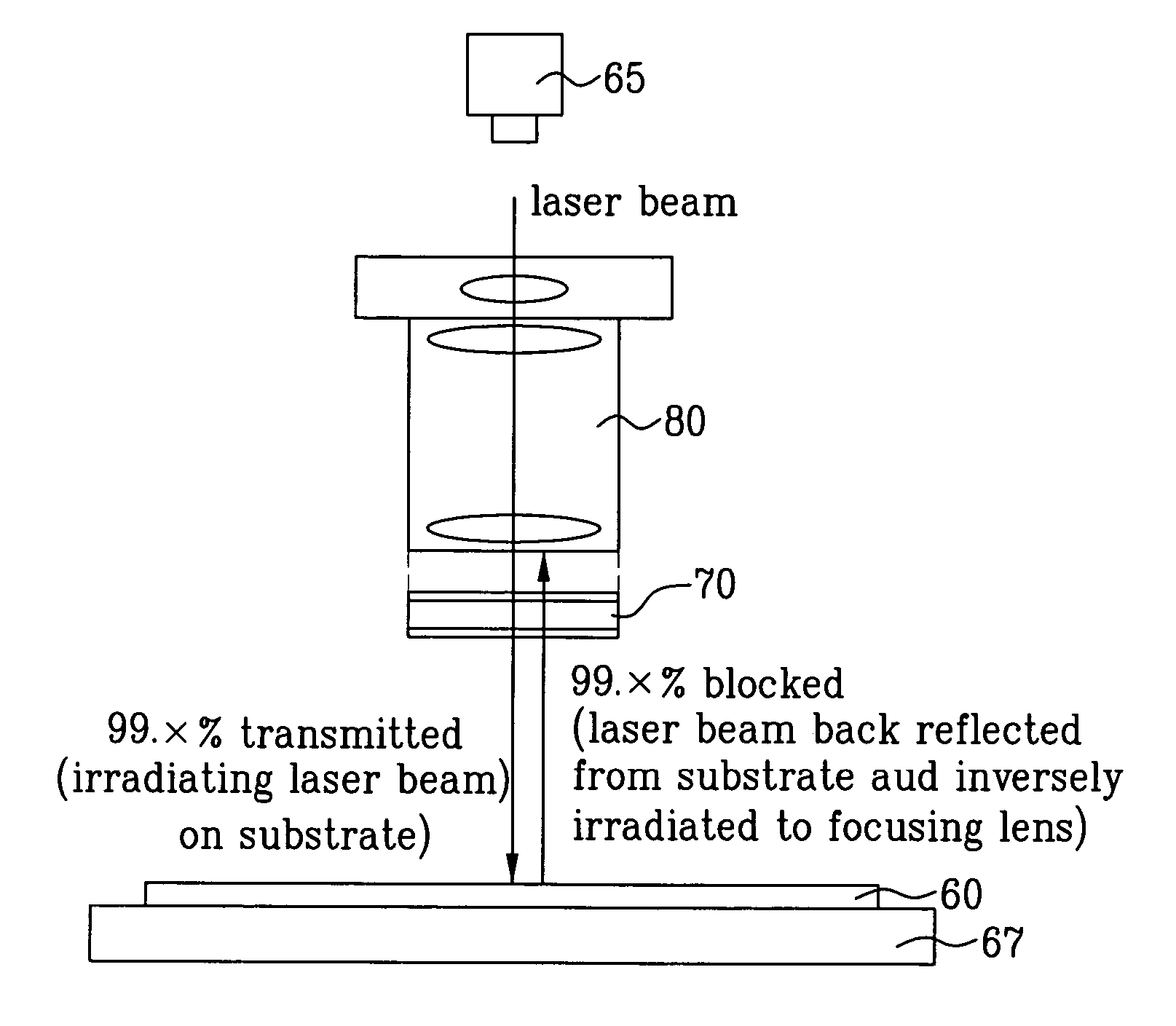
[0084]FIG. 8 illustrates a schematic view of a sequential lateral solidification device according to the present invention.

[0085]The sequential lateral solidification (SLS) device according to the present invention includes a substrate 60 having a thin silicon layer deposited thereon, a laser light source65 generating laser beams, a projection lens 80 focusing the laser beam generated from the laser light source 65, changing the pattern of the laser beam, and irradiating the laser beam having the changed pattern on the substrate 60, a laser beam splitter 70 formed below the projection lens 80, transmitting the laser beam irradiated from the laser light source 65 to the substrate 60, and blocking the laser be...


PUM

PropertyMeasurementUnit
Fractionaaaaaaaaaa

Abstract

A sequential lateral solidification device, for enhancing optical characteristics of the device and for preventing damage caused by an ablation of a crystallization thin film, is disclosed. The device includes a laser light source generating a laser beam, a projection lens focusing the laser beam generated from the laser light source onto a substrate, a laser beam splitter between the projection lens and the substrate that passes the laser beam generated from the laser light source to irradiate the substrate and that blocks the laser beam reflected back from the substrate towards the projection lens, and a stage having the substrate mounted thereon.

Description

[0001]This application claims the benefit of Korean Application No. P2003-043647, filed on Jun. 30, 2003, which is hereby incorporated by reference as if fully set forth herein.BACKGROUND OF THE INVENTION[0002]1. Field of the Invention[0003]The present invention relates to a silicon solidification device, and more particularly, to a sequential lateral solidification device. Although the present invention is suitable for a wide scope of applications, it is particularly suitable for improving optical characteristics of the sequential lateral solidification device and preventing optical damage caused by ablation of the crystallization thin film.[0004]2. Discussion of the Related Art[0005]As information technologies develop, various displays are in demand. Recently, many efforts have been made to research and develop various flat display panels such as a liquid crystal display device (LCD), a plasma display panel (PDP), an electroluminescent display (ELD), a vacuum fluorescent display (...

Claims


Application Information

Patent Timeline
IPC IPC(8): B23K26/00H01L21/324H01L21/027B23K26/06B23K26/16C30B13/24
CPCB23K26/0656B23K26/16C30B13/24B23K26/066H01L21/027
Inventor JUNG, YUN HO
Owner LG DISPLAY CO LTD
Why Eureka
Try Eureka