Process for producing highly doped semiconductor wafers, and dislocation-free highly doped semiconductor wafers

a semiconductor wafer and high-doping technology, applied in the direction of water-setting substance layered product, transportation and packaging, under a protective fluid, etc., can solve the problems of unintentionally altering the resistivity, minimum substrate resistance, and high production cost, so as to simplify the production of dislocation-free semiconductor wafers and improve the properties. , the effect of low resistan

Inactive Publication Date: 2008-03-11
SILTRONIC AG
View PDF22 Cites 7 Cited by
  • Summary
  • Abstract
  • Description
  • Claims
  • Application Information

AI Technical Summary

Benefits of technology

[0007]The present invention provides a process which makes available dislocation-free semiconductor wafers whose resistivity has decreased to values which were not hitherto possible to reach with just one defined dopant. The present invention also provides a process which makes it possible to produce dislocation-free semiconductor wafers of a defined doping (n-type or p-type) and with improved properties, and / or which simplifies the production of dislocation-free semiconductor wafers with low resistivity.

Problems solved by technology

In industrial fabrication of semiconductor elements this leads to higher production costs.
A further drawback of dopants with high diffusion coefficients results from the phenomenon known as auto-doping during the deposition of epitaxial layers.
In this phenomenon, the dopant passes out of the substrate via the gas phase into the epitaxial layer and unintentionally alters the resistivity thereof.
However, the use of large quantities of dopant in the production of single crystals has various associated problems which restrict the minimum substrate resistances that can be achieved: high dopant concentrations in the melt can lead to precipitations of the dopant in the melt and to constitutional supercooling, which in both cases prevents single-crystalline growth.
Moreover, large quantities of individual dopants may evaporate out of the melt, which increases the quantity of dopant required and can lead to the undesirable formation of toxic chemical compounds.
A further problem with high dopant concentrations is that above certain concentrations some of the dopant atoms incorporated in the semiconductor material may be electrically inactive.

Method used


Image

  • Process for producing highly doped semiconductor wafers, and dislocation-free highly doped semiconductor wafers
  • Process for producing highly doped semiconductor wafers, and dislocation-free highly doped semiconductor wafers

Examples


Embodiment Construction

)

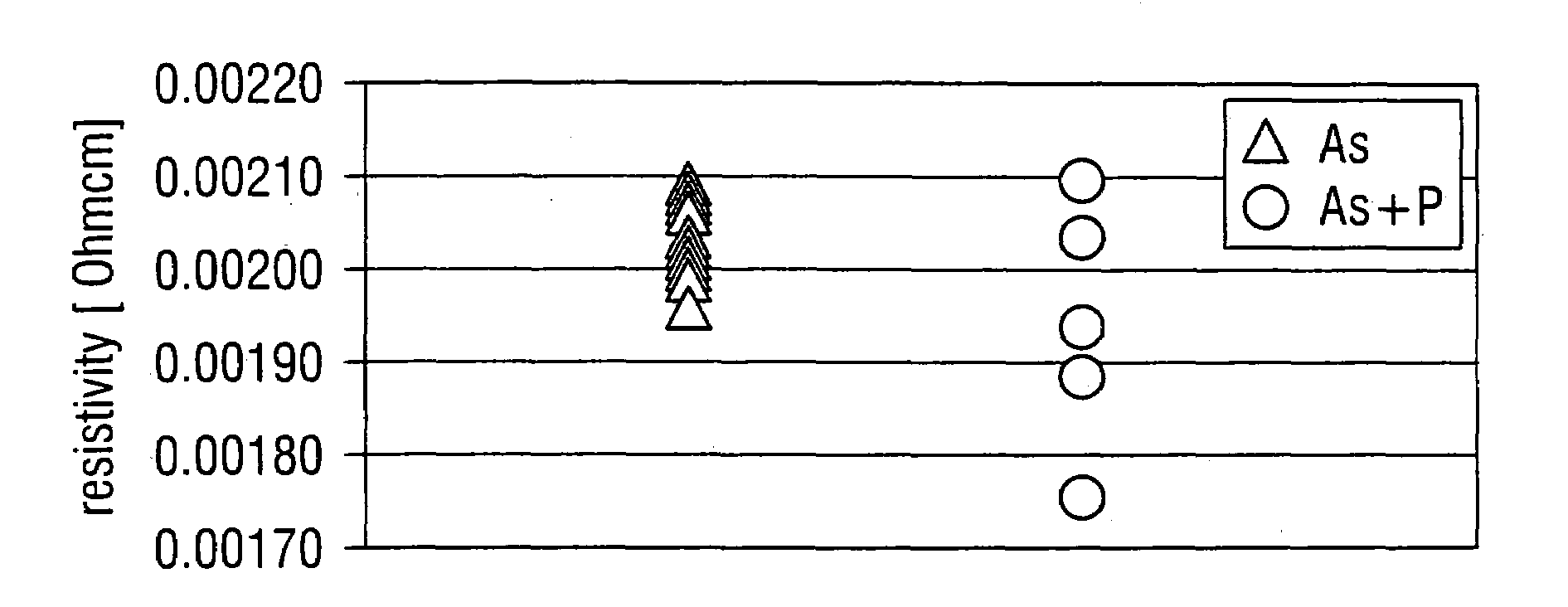
[0011]The semiconductor wafer preferably consists of silicon or germanium or a mixture of silicon and germanium and has a resistivity of 0.0005-0.1 Ohm·cm, more preferably 0.0005-0.005 Ohm·cm, and most preferably of 0.0005-0.002 Ohm·cm.

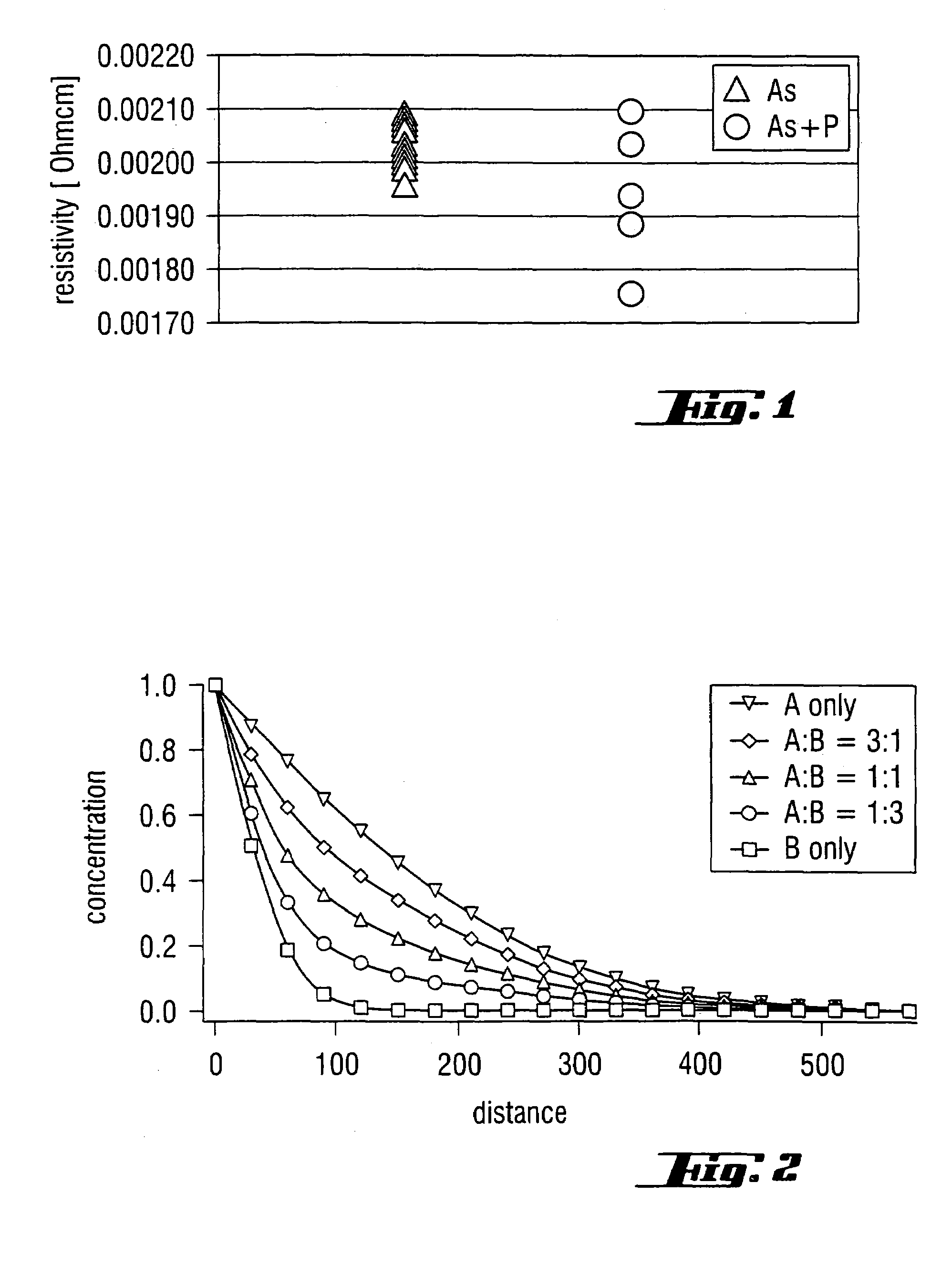
[0012]The use of a suitable combination of dopants of the same type in accordance with the present invention makes it possible to produce semiconductor substrates with improved materials properties under simplified process conditions. In the present context, dopants are considered to be of the same type if they belong to the same group of the periodic system of the elements. Although the prior art has described processes in which doping is likewise carried out using at least two different dopants, these processes differ fundamentally from the present invention in that they are in part aimed at achieving different effects and that there is no mention of doping with two electrically active dopants from the same group of the periodic system of the eleme...


PUM

PropertyMeasurementUnit
resistivityaaaaaaaaaa

Abstract

The invention relates to a process for producing highly doped semiconductor wafers, in which at least two dopants which are electrically active and belong to the same group of the periodic system of the elements are used for the doping. The invention also relates to a semiconductor wafer which is free of dislocations and is doped with at least two electrically active dopants which belong to the same group of the periodic system of the elements.

Description

BACKGROUND OF THE INVENTION[0001]1. Field of the Invention[0002]The invention relates to a process for producing highly doped semiconductor wafers, in which at least two dopants are used. The invention also relates to dislocation-free, highly doped semiconductor wafers.[0003]2. Background Art[0004]Highly doped semiconductor substrates with a low resistivity are needed, for example, for the fabrication of power components. In conventional processes, in each case, only one specific element is incorporated as a dopant in the semiconductor wafers in order to reduce the substrate resistance, for example, B, P, As, or Sb in silicon. Typical dopant concentrations for highly doped silicon are greater than 1018 / cm3, and are usually achieved by adding the dopant to the melt before or during crystal growth or through diffusion of the dopant into the semiconductor wafers which have been processed from the single crystal that has been grown.[0005]The diffusion constant of the dopant in the semic...

Claims


Application Information

Patent Timeline
Patent Type & Authority Patents(United States)
IPC IPC(8): C30B15/00B32B3/02H01L21/00B32B9/04H01L21/24C30B15/04C30B29/02C30B29/06C30B29/08C30B29/52H01L21/02H01L29/167
CPCC30B15/04C30B29/06C30B29/08H01L29/167C30B29/52Y10S438/914Y10T428/21H01L21/24
Inventor KRAUTBAUER, RUPERTGMEILBAUER, ERICHVORBUCHNER, ROBERTWEBER, MARTIN
Owner SILTRONIC AG
Why Eureka
Try Eureka