Apparatus for reducing power supply noise in an integrated circuit

a technology for reducing power supply noise and integrated circuits, which is applied in the direction of individual semiconductor device testing, liquid/fluent solid measurement, instruments, etc., can solve the problem of not having the space to mount the required number of capacitors, the inability to reduce the reactance by a large amount, and the inability to reduce the reactance. the effect of limiting the variation of power supply voltage and reducing the noise of the du

Inactive Publication Date: 2008-03-11
FORMFACTOR INC
View PDF14 Cites 73 Cited by
  • Summary
  • Abstract
  • Description
  • Claims
  • Application Information

AI Technical Summary

Benefits of technology

[0012]During a test of an integrated circuit device under test (DUT) employing synchronous logic, the DUT experiences a temporarily increase in its demand for power supply current after each pulse of a clock signal input to the DUT because each clock signal pulse initiates state transitions of clocked logic devices within the DUT. The DUT needs the extra current to charge input capacitance of transistors forming those logic devices. It is an object of the invention to provide a means for limiting variation in power supply voltage at the power input terminal of a DUT arising from the transient increase in power supply current following each clock signal pulse, thus reducing the power supply noise at the DUT.
[0013]In accordance with one aspect of the invention, a charging current is supplied to the DUT's power input terminal from an auxiliary power supply source after each clock signal pulse to supplement a current continuously supplied by a main power supply during the test. The additional charging current reduces the need for the main power supply to increase its output current to meet the DUT's increased demand. With the output current of the main power supply being held substantially constant despite the DUT's increased demand for current, any voltage drop across path impedance between the main power supply and the DUT remains substantially constant. Thus the supply voltage at the DUT's power input terminal remains substantially constant.
[0015]In accordance with a further aspect of the invention, in a preferred embodiment thereof, the auxiliary power source includes a capacitor, a transistor switch and a voltage source. The voltage source charges the capacitor before each clock signal pulse and the switch temporarily connects the capacitor to the DUT's power input terminal at the start of each clock cycle so that the capacitor can deliver its charge to the DUT to provide the DUT's required transient charging current. The voltage to which the capacitor is charged is adjusted prior to the start of each clock signal cycle so that the capacitor delivers the amount of charge the DUT is predicted to require during the next state change. The system can regulate the DUT's supply voltage even when there is significant path impedance between the capacitor and the DUT. Thus the capacitor may be mounted on a probe card relatively distant from DUT.

Problems solved by technology

However there are practical limits to the amount by which we can reduce that reactance.
Unfortunately it is not always convenient or possible to mount a large capacitor on a probe card 12 near the power supply input terminal 26 of each DUT 14. FIG. 4 is a simplified plan view of a typical probe card 12.
However when a wafer includes a large number of ICs to be tested or an IC having a large number of densely packed terminals, there is not enough space to mount the required number of capacitors C1 of sufficient size sufficiently close to central area 27.

Method used


Image

  • Apparatus for reducing power supply noise in an integrated circuit
  • Apparatus for reducing power supply noise in an integrated circuit
  • Apparatus for reducing power supply noise in an integrated circuit

Examples


Embodiment Construction

)

System Architecture

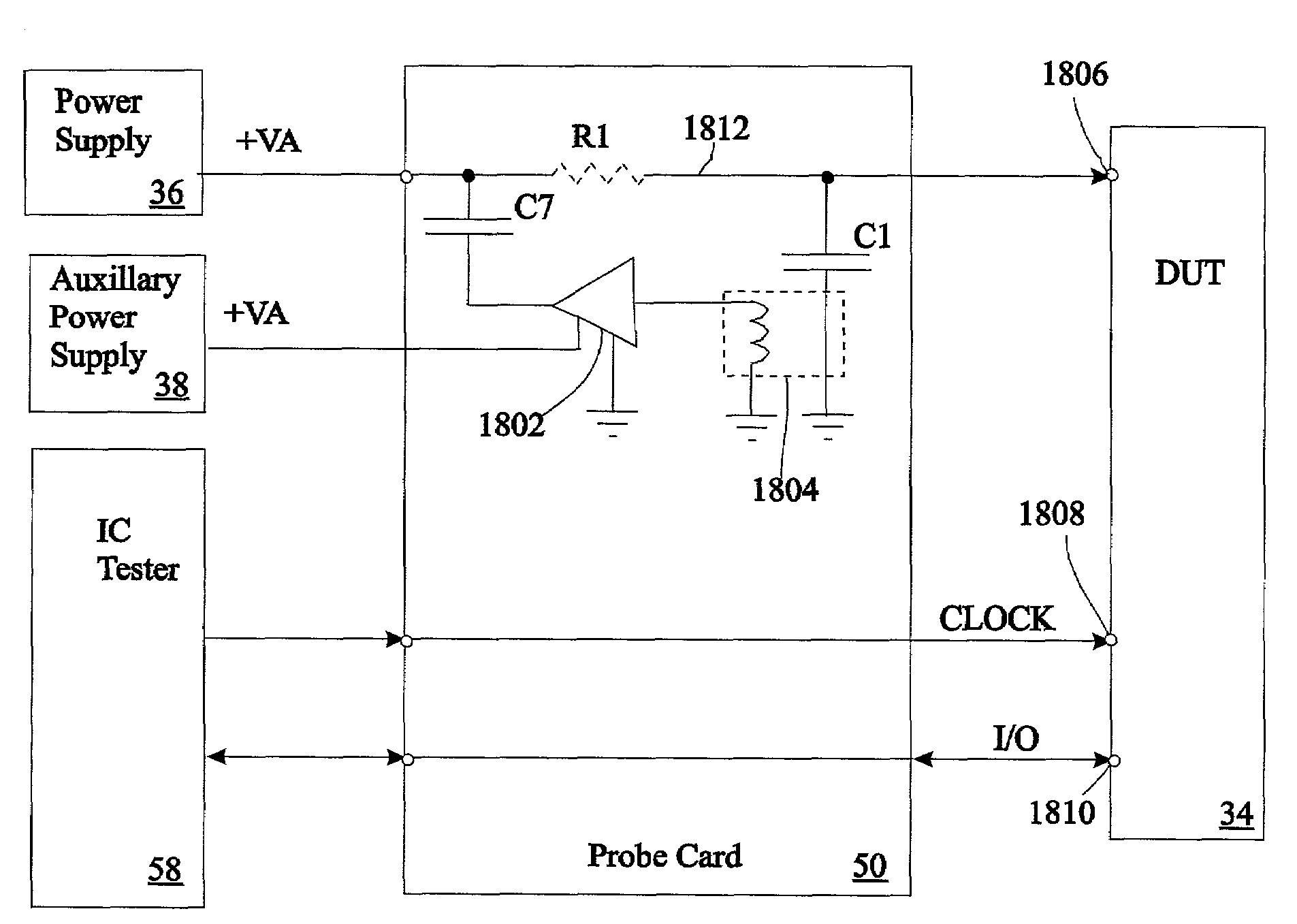
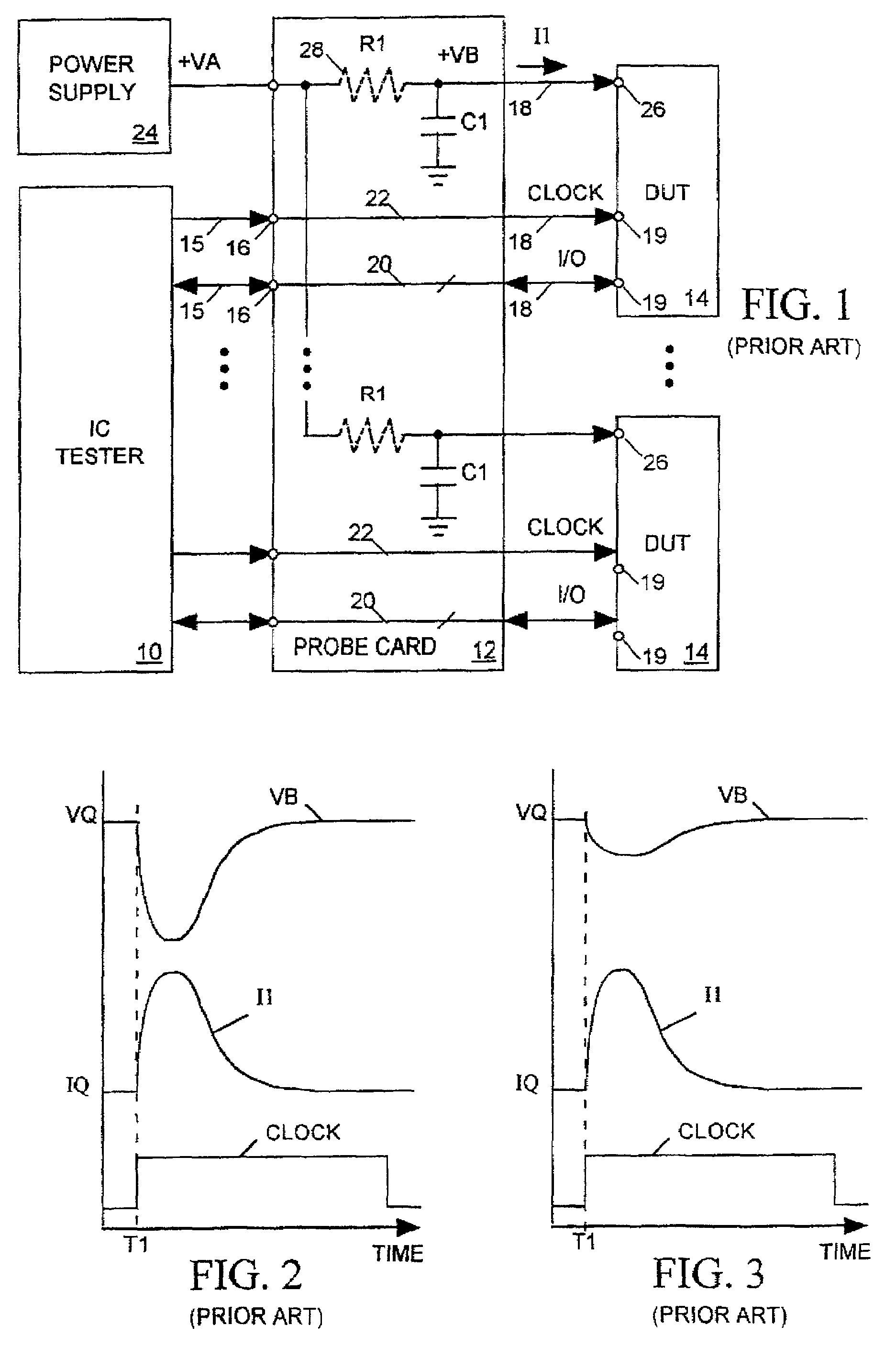
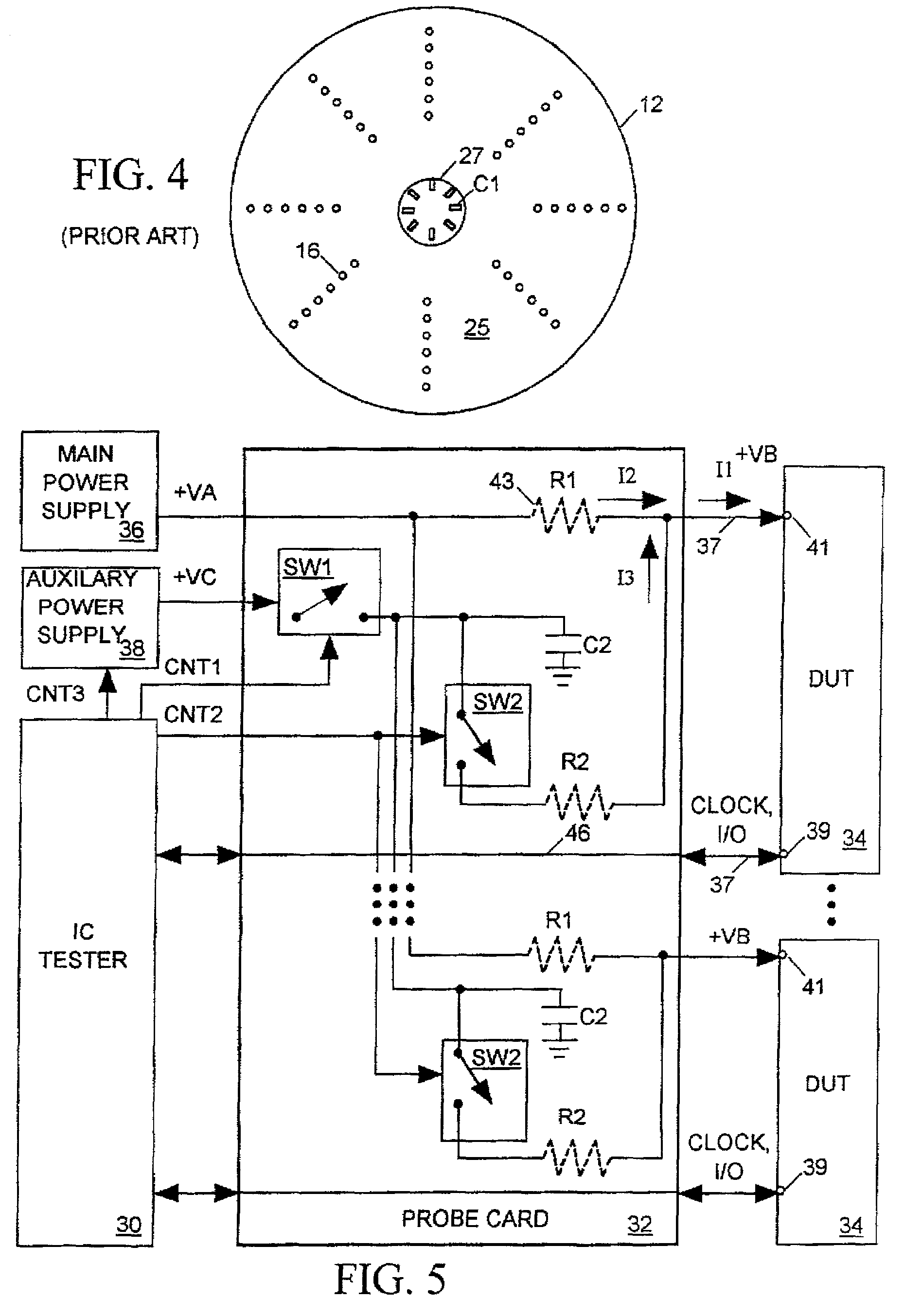
[0038]FIG. 5 illustrates in block diagram form an integrated circuit (IC) tester 30 linked through a probe card 32 to a set of similar IC devices under test (DUTs) 34 in the form of die on a semiconductor wafer. Probe card 32 includes a set of probes 37 for accessing input / output terminal pads 39 on the surfaces of DUTs 34 and also includes signal paths 46 linking tester 30 to probes 37 to allow IC tester 30 to send a clock signal (CLOCK) and other test signals to DUTs 14 and to convey DUT output signals back to tester 30 so that the tester can monitor the behavior of the DUTs.

[0039]Probe card 34 also links a main power supply to a power input terminal 41 of each DUT 34 via probes 37. Power supply 36 produces a well-regulated output voltage VA and continuously supplies a current I2 to DUT 34. For illustrative purposes, FIG. 5 represents the inherent impedances of the paths 43 through probe card 32 between main power supply 36 and each DUT 34 as resistors R1. Due ...


PUM


Abstract

A power supply provides power to a power terminal of an integrated circuit device under test (DUT). The DUT's demand for current at the power input terminal may temporarily increase due, for example, to state changes in the DUT. To limit variation (noise) in voltage at the power input terminal, a supplemental current is supplied to the power input terminal.

Description

CROSS-REFERENCE TO RELATED APPLICATIONS[0001]This application is a continuation-in-part of U.S. application Ser. No. 10 / 003,596, filed Oct. 30, 2001, which is a divisional of U.S. application Ser. No. 09 / 484,600, filed Jan. 18, 2000, now U.S. Pat. No. 6,339,338 B1.BACKGROUND OF THE INVENTION[0002]1. Field of the Invention[0003]The present invention relates in general to systems for testing integrated circuits and in particular to an apparatus for reducing power supply noise in an integrated circuit under test resulting from state transitions of the logic it implements.[0004]2. Description of Related Art[0005]An integrated circuit (IC) tester can concurrently test a set of ICs in the form of die on a silicon wafer. FIG. 1 is a block diagram illustrating a typical IC tester 10 connected through a probe card 12 to a set of similar IC devices under test (DUTs) 14. Tester 10 uses pogo pins 15 or other means to connect various input and output terminals to a set of contacts 16 on probe ca...

Claims


Application Information

Patent Timeline
Patent Type & Authority Patents(United States)
IPC IPC(8): G01R31/26G01R31/28G01R31/317G01R31/319G06F1/26
CPCG01R31/31721G06F1/26G01R31/2851G01R31/31905G01R31/31924
Inventor ELDRIDGE, BENJAMIN N.MILLER, CHARLES A.
Owner FORMFACTOR INC
Why Eureka
Try Eureka