Substrate for optical element, organic electroluminescence element and organic electroluminescence display device
a technology of organic electroluminescence and substrate, which is applied in the direction of luminescence screens, identification means, instruments, etc., can solve the problems of lumonous efficiency over the limit, and the efficiency of light extraction is fatally affected by performance degradation
- Summary
- Abstract
- Description
- Claims
- Application Information
AI Technical Summary
Benefits of technology
Problems solved by technology
Method used
Image
Examples
example 1
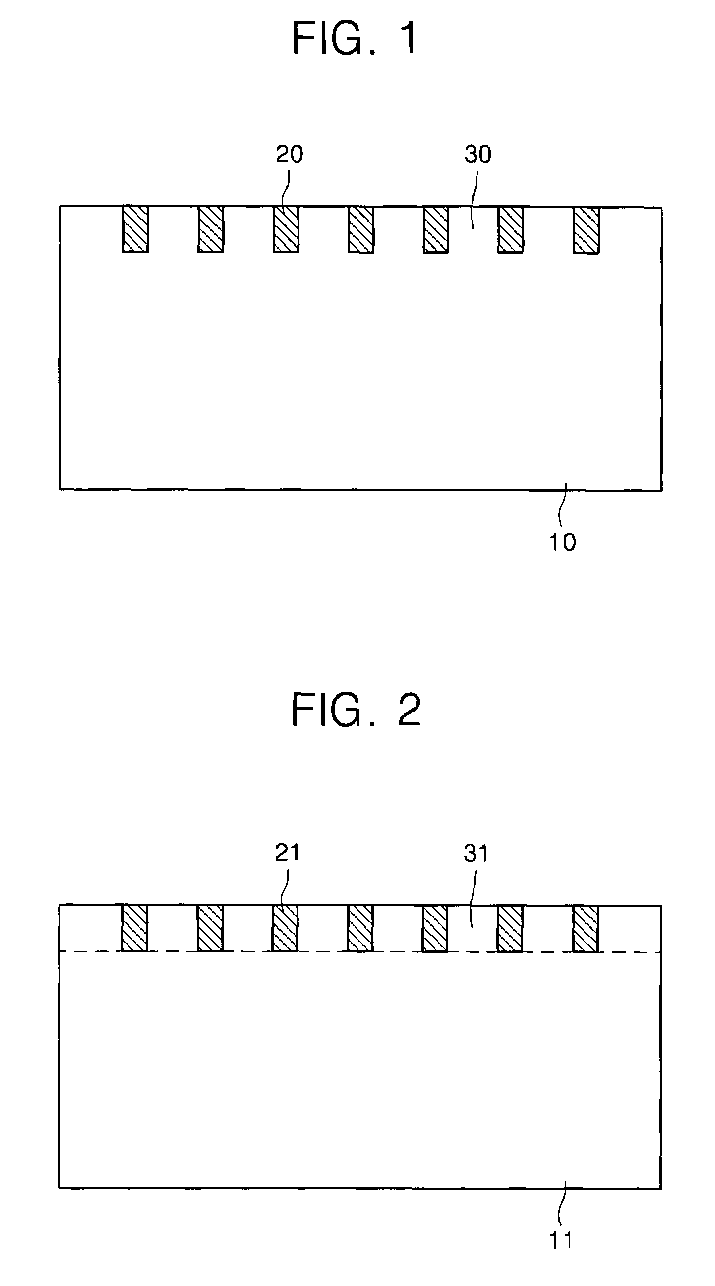
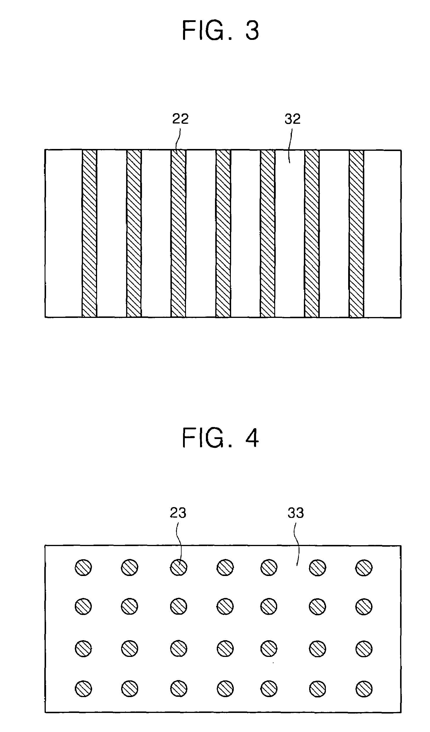
[0073]A positive resist material was formed on the quartz substrate (refractive index: 1.457) in a thickness of 4000 μm using a spin coater, as a photoresist material, and then the resist material was patterned using a photomask.
[0074]As a light source, an Hg—Xe lamp (wavelength: 250 nm) was used. Here, a stripe type mask pattern was used with a period of 1.0 μm, a line width of 0.75 μm, and a space width of 0.25 μm. With this mask, after exposed one time, the mask was rotated 90°, and was exposed again with the same condition. After such exposure, the mask was processed with alkali developer to form the resist pattern. As a result of SEM observation, it was confirmed that a target grating pattern could be manufactured. The quartz substrate attached to the manufactured resist pattern was etched by reactive gas etching (Samuco, RIE1ONR). Etching was performed under the condition of 100 W output, using CF4(4 Pa, 20 SCCM). The etching was performed to make a groove of 10000 μm in the q...
example 2
[0079]A positive resist material was formed on the quartz substrate (refractive index: 1.457) in a thickness of 4000□ by a spin coater, as a photoresist material, and then the formed photoresist layer was exposed by two-optical-flux laser interference exposure system. As a laser light source used in this two-optical-flux laser interference exposure, an Ar-ion laser (wavelength: 488 nm) was employed to make exposure under the following conditions.
[0080]Laser light was branched into 2 light flux with a beam splitter, and interference exposure was performed with a mirror such that a crossing angle becomes about 31 degree on the substrate surface (laser illumination intensity: 100 mA / μm, exposure time: 15 seconds). After such exposure was performed one time, the substrate was rotated 90° and exposed again with the same condition.
[0081]After exposure, it was processed by alkali developer AZ300MIF (manufactured by Clariant Japan Co.) to form the grating pattern. As a result of SEM observa...
PUM
 Abstract
Description
Claims
Application Information


