Method of measuring three-dimensional surface roughness of a structure

a three-dimensional surface roughness and structure technology, applied in the direction of material analysis using wave/particle radiation, instruments, photomechanical equipment, etc., can solve the problems of large tolerance budget, adversely affecting the performance of a finished semiconductor device, and consuming a large amount of processing error margin, etc., to achieve accurate measurement, more accurate information of feature profiles, and great precision

Inactive Publication Date: 2008-03-25
FEI CO
View PDF5 Cites 62 Cited by
  • Summary
  • Abstract
  • Description
  • Claims
  • Application Information

AI Technical Summary

Problems solved by technology

As design rules shrink, the margin for error in processing becomes smaller.
Even small deviations from design dimensions may adversely affect the performance of a finished semiconductor device.
Characteristics such as profile roughness, such as roughness along the bottom of trenches or on the sidewalls of lines, which could be ignored for larger features, now consumes a large amount of the tolerance budget.
However, the resolution of optical methods is limited, typically greater than 0.5 micron, and such methods do not directly measure surface topography.
However, mechanical profilers are typically very slow.
Resolution is limited by the size of the probe or stylus, and very small probes are difficult to manufacture and are very fragile.
Also, measurement of features with high-aspect ratios or undercut surfaces is very difficult using any type of stylus profilometer.
The SEM alone, however, can only view a feature from the top down.
While overall roughness can be measured, it is very difficult to determine whether the roughness is at the bottom or top of the feature.
Further, the SEM, like the optical and mechanical methods discussed above, can only be used to measure surface features.
The profile roughness of buried features or features surrounded by other materials cannot be measured using these methods.

Method used


Image

  • Method of measuring three-dimensional surface roughness of a structure
  • Method of measuring three-dimensional surface roughness of a structure
  • Method of measuring three-dimensional surface roughness of a structure

Examples


Embodiment Construction

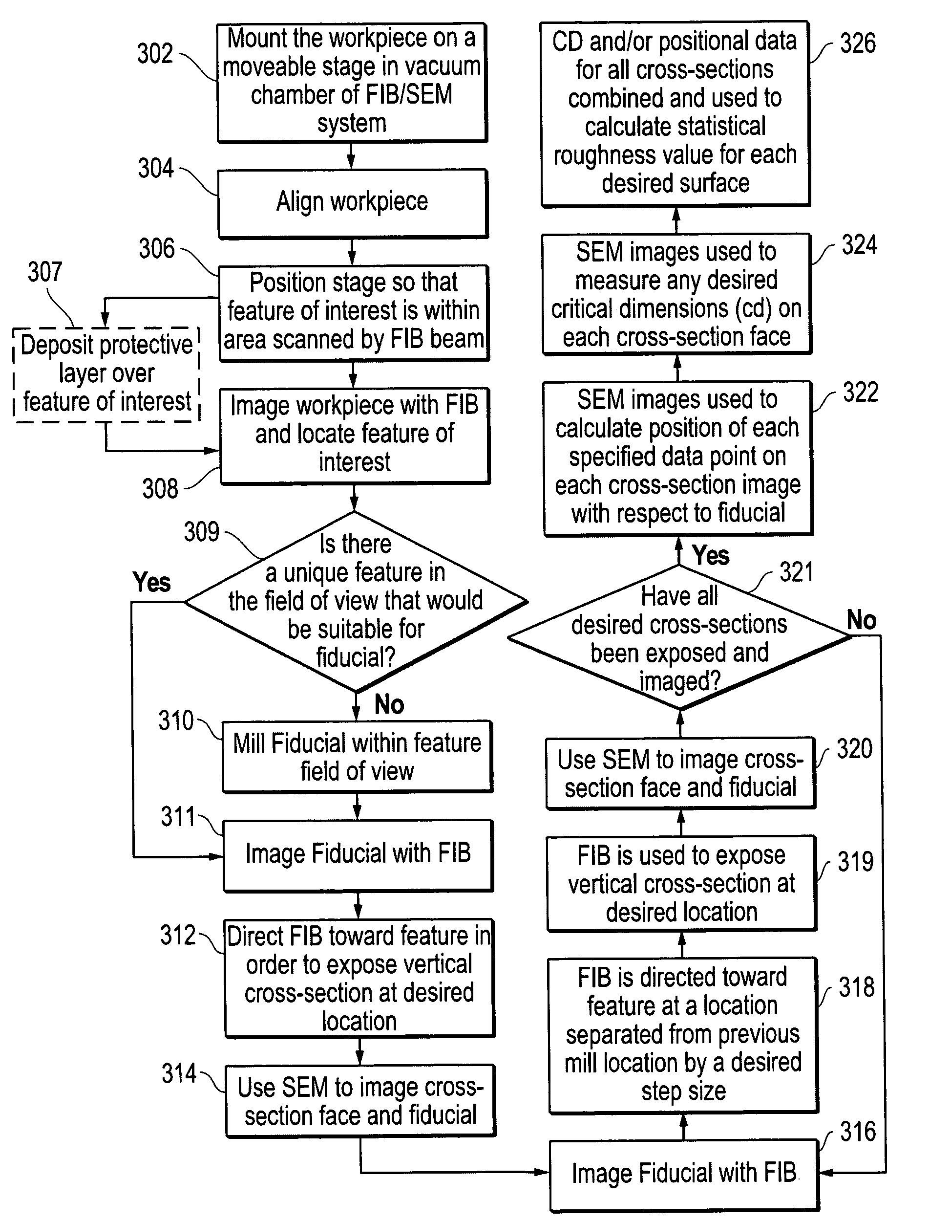
[0036]Preferred embodiments of the present invention are directed to methods and an apparatus for measuring the three-dimensional surface roughness of a structure or feature. In a preferred embodiment of the present invention, the sample to be measured is loaded into a dual beam FIB-SEM. The FIB is used to mill a succession of cross-sections or “slices” of the feature of interest at pre-selected intervals over a pre-selected measurement distance. As each cross-section is exposed, the SEM is used to measure the relevant dimensions of the feature. Data from these successive “slices” is then used to determine the three-dimensional surface roughness for the feature.

[0037]Although much of the following description is directed toward the measurement of the width of a structure, the methods of the present invention are equally applicable to any relevant dimension, including height, slope, sidewall angle, etc. Further, although much of the following description is also directed toward the u...


PUM


Abstract

An improved method of measuring the three-dimensional surface roughness of a structure. A focused ion beam is used to mill a succession of cross-sections or “slices” of the feature of interest at pre-selected intervals over a pre-selected measurement distance. As each cross-section is exposed, a scanning electron microscope is used to measure the relevant dimensions of the feature. Data from these successive “slices” is then used to determine the three-dimensional surface roughness for the feature.

Description

[0001]This application claims priority from U.S. Provisional Application No. 60 / 700,654, filed on Jul. 19, 2005.TECHNICAL FIELD OF THE INVENTION[0002]The present invention relates to charged particle beam processing and, in particular, to a method of determining three-dimensional surface roughness for a structure.BACKGROUND AND SUMMARY OF THE INVENTION[0003]Semiconductor manufacturing, such as the fabrication of integrated circuits, typically entails the use of photolithography. A semiconductor substrate on which circuits are being formed, usually a silicon wafer, is coated with a material, such as a photoresist, that changes solubility when exposed to radiation. A lithography tool, such as a mask or reticle, positioned between the radiation source and the semiconductor substrate casts a shadow to control which areas of the substrate are exposed to the radiation. After the exposure, the photoresist is removed from either the exposed or the unexposed areas, leaving a patterned layer ...

Claims


Application Information

Patent Timeline
Patent Type & Authority Patents(United States)
IPC IPC(8): H01J37/30
CPCG01B15/08G01N23/2251G03F7/70625
Inventor CHITTURI, PRASANNAHONG, LIANGHENRY, CRAIGNOTTE, JOHN
Owner FEI CO
Why Eureka
Try Eureka