Low voltage sensing scheme having reduced active power down standby current

a low voltage sensing and active power technology, applied in static storage, information storage, digital storage, etc., can solve the problems of reducing the transistor threshold voltage, increasing the transistor off current, and increasing the standby power consumption, so as to reduce the active power down standby leakage current and low voltage

Active Publication Date: 2008-05-13
MICRON TECH INC
View PDF14 Cites 41 Cited by
  • Summary
  • Abstract
  • Description
  • Claims
  • Application Information

AI Technical Summary

Benefits of technology

[0025]The present disclosure thus describes a low voltage sensing scheme that reduces active power down standby leakage current in a memory device. During memory's active power down state, the leak current may increase because of the use of P and Nsense amplifiers having low threshold voltages (Vth) for low Vcc sensing of data signals. A clamping device or diode is used between a Psense amplifier control line (e.g. ACT) and Vcc and / or between an Nsense amplifier control line (e.g. RNL*) and Vss (ground potential). The clamping diode is not enabled during normal memory operations, but is turned on during active power down mode to reduce leakage current through ACT and / or RNL* nodes. The clamping device connected to the ACT node may reduce the voltage on the ACT line during power down mode, whereas the clamping device connected to the RNL* node may increase the voltage on the RNL* line during power down mode to reduce sense amplifier leakage current through these nodes. The voltages on ACT and RNL* lines go back to their original levels when the memory device exits the power down mode. Clamping devices can be implemented without significant modifications to the sense amplifier layout in a memory chip and without any complex data loss prevention measures.

Problems solved by technology

However, such low supply voltage operation requires reducing the transistor threshold voltages (Vth).
But, reducing the transistor threshold voltage (Vth) results in increased transistor off current and higher standby power consumption.
A low threshold (Vth) transistor in the sense amplifier circuit may produce a relatively big leak current when the sense amplifier is activated (for example, during a memory's active state or power-down state).
However, such configuration requires periodically exiting the power down mode and performing frequent burst refresh cycles in the memory device to prevent data loss.
However, these prior art methods are cumbersome and complicated to implement.
These methods may also result in additional memory circuitry to perform various monitoring and control functions, thereby increasing the chip real estate.

Method used


Image

  • Low voltage sensing scheme having reduced active power down standby current
  • Low voltage sensing scheme having reduced active power down standby current
  • Low voltage sensing scheme having reduced active power down standby current

Examples


Embodiment Construction

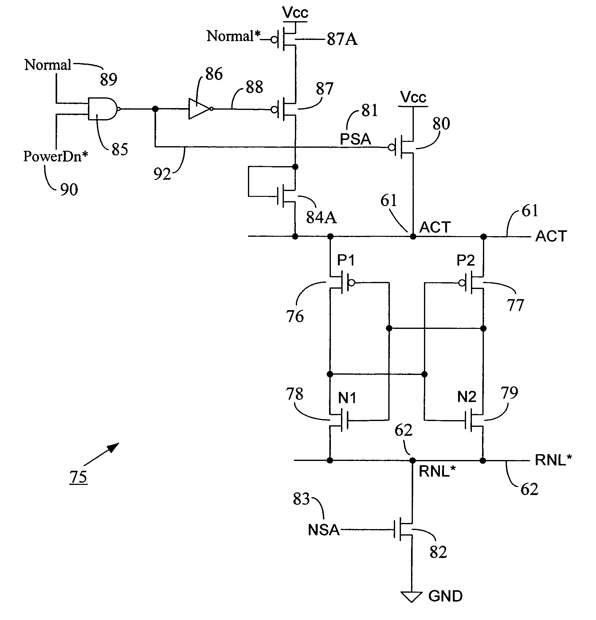
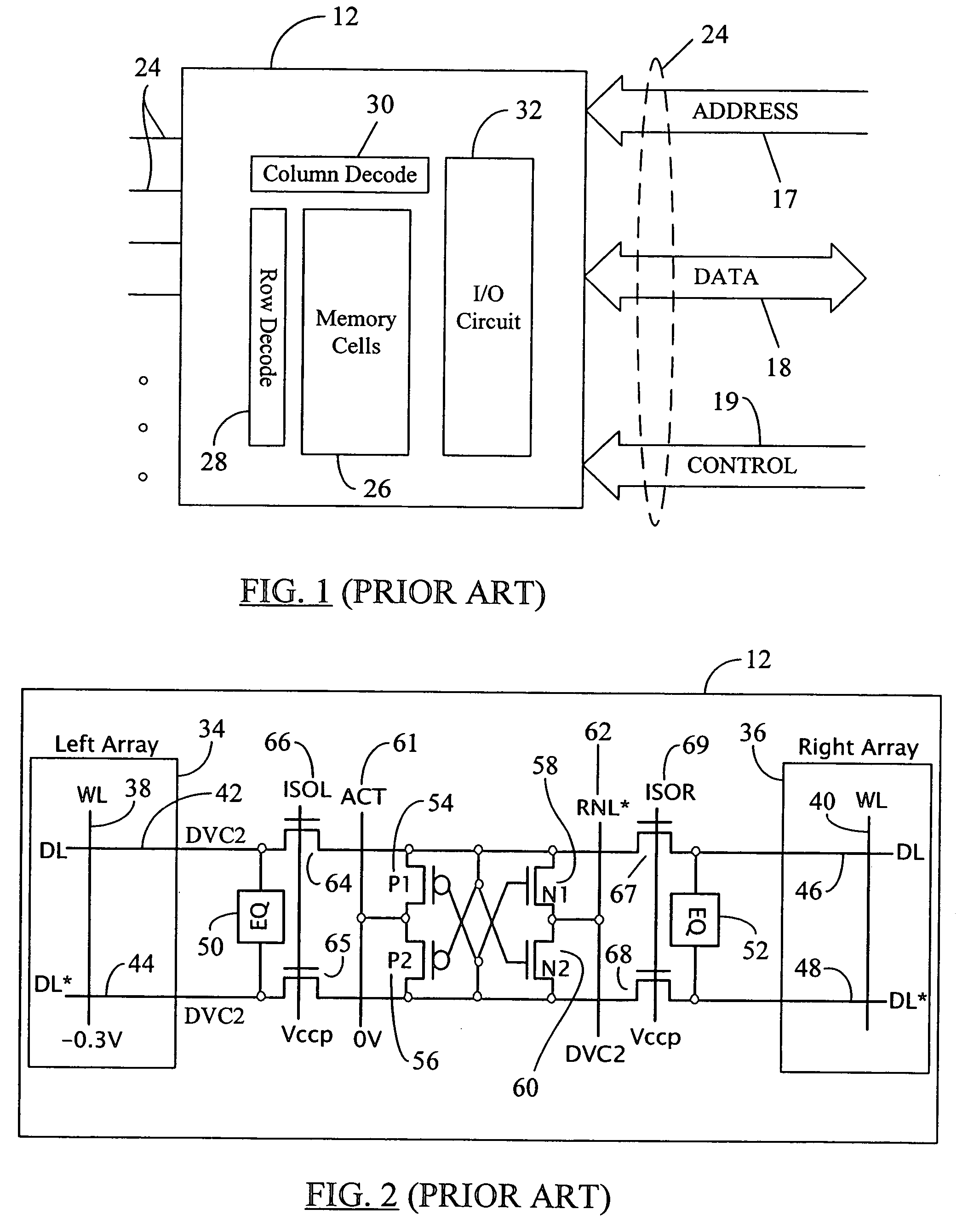
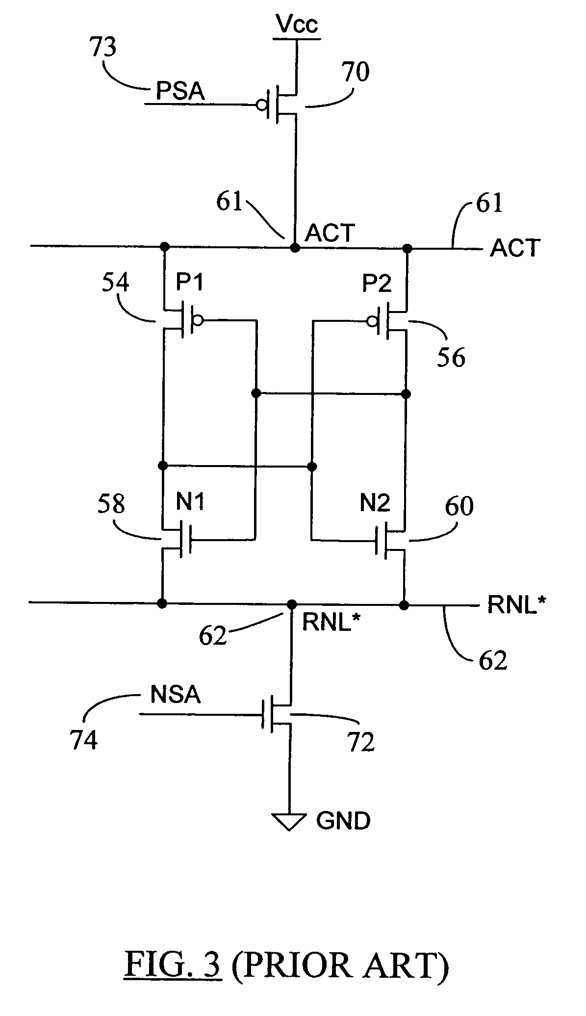
[0037]Reference will now be made in detail to certain embodiments of the present disclosure, examples of which are illustrated in the accompanying drawings. It is to be understood that the figures and descriptions of the present disclosure included herein illustrate and describe elements that are of particular relevance to the present disclosure, while eliminating, for the sake of clarity, other elements found in typical solid-state electronic devices, memories or memory-based systems. It is noted at the outset that the terms “coupled,”“connected”, “connecting,”“electrically connected,” etc., are used interchangeably herein to generally refer to the condition of being electrically connected. It is further noted that various block diagrams and circuit diagrams shown and discussed herein employ logic circuits that implement positive logic, i.e., a high value on a signal is treated as a logic “1” whereas a low value is treated as a logic “0.” However, any of the circuits discussed here...


PUM


Abstract

A low voltage sensing scheme reduces active power down standby leakage current in a memory device. During memory's active power down state, the leak current may increase because of the use of P and Nsense amplifiers having low threshold voltages (Vth) for low Vcc sensing of data signals. A clamping device or diode is used between a Psense amplifier control line (e.g. ACT) and Vcc and / or between an Nsense amplifier control line (e.g. RNL*) and Vss (ground potential). The clamping diode is not enabled during normal memory operations, but is turned on during active power down mode to reduce leakage current through ACT and / or RNL* nodes. The clamping device connected to the ACT node may reduce the voltage on the ACT line during power down mode, whereas the clamping device connected to the RNL* node may increase the voltage on the RNL* line during power down mode to reduce sense amplifier leakage current through these nodes.

Description

BACKGROUND[0001]1. Field of the Disclosure[0002]The present disclosure generally relates to electronic devices and, more particularly, to a system and method to substantially reduce active power down standby current in semiconductor memory chips.[0003]2. Brief Description of Related Art[0004]Memory devices are electronic devices that are widely used in many electronic products and computers to store data. A memory device is a semiconductor electronic device that includes a number of memory cells, each cell storing one bit of data. The data stored in the memory cells can be read during a read operation. FIG. 1 is a simplified block diagram showing a memory chip or memory device 12. The memory chip 12 may be part of a DIMM (dual in-line memory module) or a PCB (printed circuit board) containing many such memory chips (not shown in FIG. 1). The memory chip 12 may include a plurality of pins or ball contacts 24 located outside of chip 12 for electrically connecting the chip 12 to other ...

Claims


Application Information

Patent Timeline
Patent Type & Authority Patents(United States)
IPC IPC(8): G11C7/10
CPCG11C7/08G11C11/4091G11C2207/2227G11C2207/065G11C5/148G11C7/06G11C7/062G11C7/065G11C7/1006G11C7/12G11C7/22
Inventor KIM, TAE
Owner MICRON TECH INC
Why Eureka
Try Eureka